This thread has been locked.

If you have a related question, please click the "Ask a related question" button in the top right corner. The newly created question will be automatically linked to this question.

The replacement inverter IC for SN74LVC1G97

Other Parts Discussed in Thread: SN74LVC1G97, SN74LVC1GU04

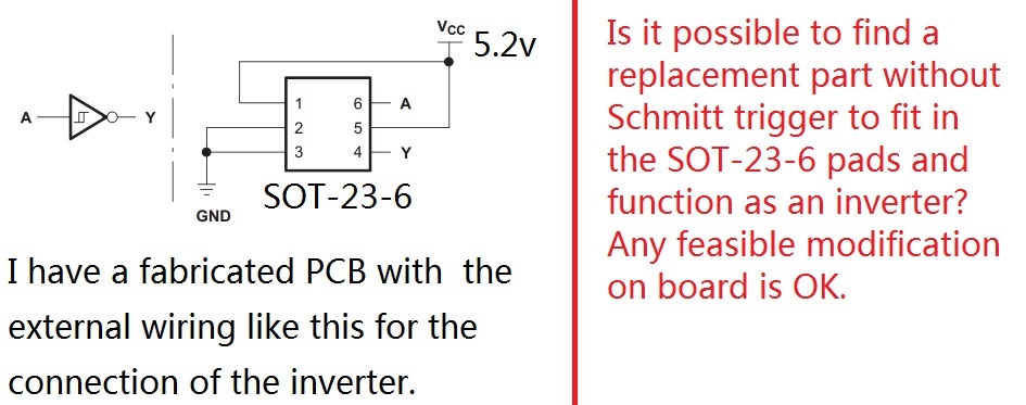
Hi, I am using SN74LVC1G97 (Configurable Multiple-Function Gate) by configuring it to the inverter. I am looking for a similar product without Schmitt triggers in the inverters to replace SN74LVC1G97. Ideally, I am looking for a part with identical footprint and pin configurations, so I can replace SN74LVC1G97 in my fabricated PCB. If this is not possible, would you give me some suggestions of the product that I can use to keep my PCB and minimize the board modification?

Thank you!

  • Hello Yi,

    Is there a reason why you don't want the schmitt trigger inputs for the device?
    These inputs mostly help with noise and slow rising inputs.

    I have gone ahead and prefiltered a list of parts for you that may work for your application.
    Assuming 5V Vcc, no schmitt trigger, S0T-23, and a single inverter gate
    Parametric search results.

    Hopefully this should help, please let me know if you have additional questions.

    Best,
    Michael

  • Hi Michael, thank you for your advise! I have recognized that I do not necessarily need this feature now. A different question will be asked in this forum.
  • Hi Michael,

    I have gone through the parts in the list that you provided. Unfortunately, none of them have pin compatibility with my exsiting pcb. Is it possible to find one part (maybe not single invter, but the configurable logic circuits) to have a non-hystresis inverter, when pin 6 is the input, pin 4 is the output, either or both of pin 1 and 5 are connected to Vcc, either or both of pin 2 and 3 to GND?
  • Hi YI,

    I'm afraid that your initial selection of part did not have a standard inverter pinout -- it is a configurable logic device. Any standard inverter will have the same pinout as the selection of devices that Michael initially provided. They are made that way on purpose to be interchangable.

    Is the Schmitt-trigger input of this device causing problems for your design? Or is this an issue of cost? I would assume that modifying a board or changing parts after going into production would be very detrimental and you would only be doing this due to a flaw in the design or a severe cost issue.
  • Hi Emrys, I am biasing the inverter in its linear mode and thus the Schmitt trigger is not preferred.  

  • I would recommend choosing an unbuffered inverter in this case, since other inverters have multiple stages and won't really do what you want.  You can search on our site for "U04" to find all parts that are unbuffered inverters.  One example is the SN74LVC1GU04

  • Can you explain to me in more details why the multiple buffer stages won't really do the linear biasing work?
  • A single inverter is designed to have a huge gain - the goal is to hit the rails on the output even when the input is just slightly above or below the input threshold values.  This means that the output voltage from a single unbuffered inverter will have an inverse correlation to the input voltage, but only through a small set of voltages near the threshold voltage (usually Vcc/2).  Adding a second and third inverter (buffering the device) will multiply the total gain, so instead of having a single huge gain, AV, you now have a gain of AV3. Many inverters have more than just 3 stages due to many different issues in design (capacitance, speed, drive strength, etc), and as such have even larger gains.

    Your best bet for driving one of these in the linear region is to use an unbuffered inverter -- which is literally just a push-pull inverting CMOS amplifier.

  • Thank you Emrys. I am a little confused about the gain of  AV3. It seems like with a higher gain mean we can use even smaller input amplitude above the threshold to get the output square wave. Why we still prefer one Av instead of its orders? Or is it because using buffers can shift the inverter from operating in the ideal linear region? 

  • It depends on what you are trying to do... I guess we are talking about two different things.
  • Sorry for the confusion. I am trying to understand the difference of the linear biasing condition when we have unbuffered inverter and buffered one.
    If placing a resistor across the unbuffered inverter can set the DC level of both input and output equal, what will be the case when we place the resistor across the input and output of the buffered inverter?
  • It's possible that it will work exactly as you expect -- I don't know of any applications where this is useful, so I have never built a circuit with this. I have just seen many engineers come to us looking for unbuffered inverters for linear buffer applications (such as oscillator drivers).

    If you would care to share your application, I would be interested to learn more about how this will be helpful to you.