Other Parts Discussed in Thread: SN74AUP1G98, SN74HCS00, SN74LVC2G132
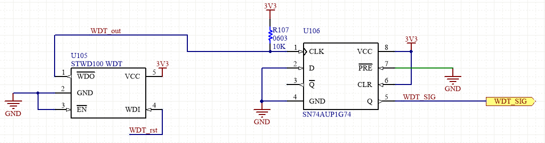
Hello, I intend to make a modified WDT circuit using SN74AUP1G74 to maintain WDT output signal low after WDT timeout event.
Most WDT dedicated circuits implement pulsating output after WDT event, but in my application I need a logic signal steady in 0V (0V on WDT_SIG will keep running a FAN until human intervention).
So, at start, we need a logic 1 on SN74AUP1G74 output (thus the /PRE pin tied to GND), and only after WDT timeout, the WDT pulses will trigger the flipflop's clock to output the desired 0V output
My concern is that during power up, the rising signal on CLK might be considered as a clock transition, and data latched to output. I understand that this component has a preset pin specifically for this scenario, but I could not find any specific timing information for this case: how long until valid VCC on flip flop will it take to a variation of CLK pin is considered a "valid edge transition"