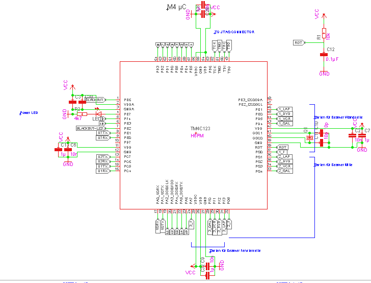
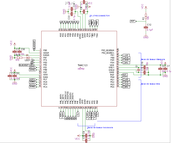
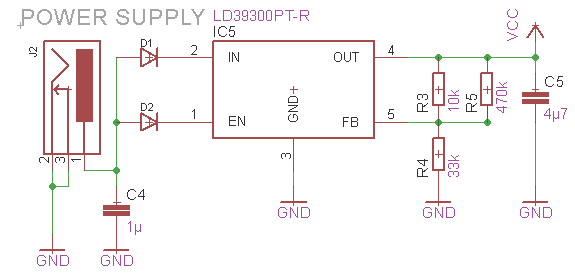
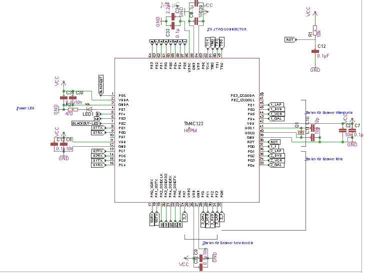
This thread has been locked.

If you have a related question, please click the "Ask a related question" button in the top right corner. The newly created question will be automatically linked to this question.

Standard schematic for Cortex M4

Hi,

I've never used a ARM. Now i want to use it and program the µC with a Stellaris Launchpad.

Can you help me and take a look of my schematic if everything is right.? Especially with the powercircuit and do i only need the standard JTAG Pins ?

TCK
TMS
TDO
TDI
RST 

I remember that for a MSP430  i need the TEST pin.....

Best regards
David


  • We have a comprehensive document on recommended layout and board design for TM4C123 device which is covered in the "System Design Guidelines for the TM4C123x Family of Tiva™ C Series Microcontrollers" found here: http://www.ti.com/lit/an/spma059/spma059.pdf

    Section "3.5 Power" covers the basic power connections needed.  

    The need for JTAG pins is based on what your design requires but I am guessing you will need access to them to program and debug any initial designs.

  • Hi David,

    A good resource for you to check your circuit against is the Tiva TM4C123 LaunchPad circuit, which can be found at http://www.ti.com/lit/ug/spmu296/spmu296.pdf . 

    The Tiva Launchpad uses a 10nF + 0.1uF capacitor combination for each of VDD and VDDA.

    Please note that VDDC should not be connected to 3.3V. It is actually an output for an internal 1.8V generator and should be connected to a 0.1uF, 1.0 uF and 2.2 uF capacitor combination to provide its filtering requirements. Repeat, do not connect VDDC to VDD.

    R2 is way too small to light up the LED. At 4.7k, you will only get 0.3 mA through the LED! A better value for R2 is 330R, which will provide a 3.9 mA drive current. The GPIO pins can provide 2, 4 or 8 mA of drive current. You can either leave it at the default, which means that you will only get 2 mA, which should be enough to just see the LED, or you can program the GPIO pin to deliver 4 mA.

    The JTAG signals are enough as shown.

    You don't need C12 (or make it DNF). Not sure where your RST signal is going to, but to theJTAG connector and a push button switch would be ideal.

    You should also provide a large capacitor (2.2 uF or more) at one location for the board's VCC supply.

    Regards, Vito

  • THANK YOU !

    Your post was very helpful i changed the things. The both user guides are very helpful!

    Here are my new schematic.

    I put a button in the near of my JTag connector ( not shown ). 

  • Hi David,

    D1 should be located to "the left" of C4 (and IN and EN shorted together). You need C4 as close as possible to IN and having a diode between C4 and IN will cause problems. I assume the diode is to prevent reverse input voltage polarity damage. I would put two diodes directly to "the right" of pin 1 of each of your power connectors. This way you get reverse voltage protection and, should J1 and J2 both be connected, you prevent one power supply feeding into the other. Although the LD39300PT-R can handle voltages as low as 2.5V and has a drop off voltage less than 0.4V, I would put in Schottky diodes to get lower voltage drops (minor consideration).

    C22 and R5 confuse me. What is their purpose?

    I assume you are after a 3.3V output, but R5's influence will make the output voltage 3.67V. R5 needs to be removed.

    The LD3900 likes R4 to be close to 4.7k. Therefore R3 would need to be 9.776k, which could be done by using a 10k in parallel with 470k combination. These resistors should be 1% tolerance.


    Not sure where X5 goes to, so its effect cannot be evaluated.


    C12 and a push button combination can be a problem. When the push button is pressed, C12 discharges with high current which can cause push button problems. The simplest solution is to remove C12 (as per the Tiva TMC123 LaunchPad). If you would like C12 to be included then there needs to be a current limiting resistor between C12 and the push button (100 ohms as per LM3S9D96 Development Board).

    Regards, Vito

  • Hello again, 

    @ Vito It's a little bit late for a thank you but i haven't time for my project because of exams. 

    Now i restarted :)

    You are totally right with your enhancements. I have changed my schematic. 

    Best regards,

    David

  • If you are wondering why i used so many Uarts. 
    I want to develop a control unit for 3 beamers which are controled by rs232c

    Best regards,

    David 

  • Hi David,

    R4 needs to be changed to 4.7k. Also, R3, R4 and R5 should be 1% resistors.

    For IC5, the IN and EN pins need to be shorted together. Also C4 needs to be on the other side of D1/D2. You only need one diode. Basically, you would have, from left to right: J2 then D1 then IC5 (pin 1 and 2). C4 is connected to IC5's pin 1/pin 2.

    It's hard to see the second drawing, so I could miss something.

    The capacitors off VDDC, according to the datasheet, should be between 2.5 to 4.0 uF. So adding a 1.0 uF capacitor would be good. Having said that, what you have would work fine.

    There is no mechanism to reset the micro. A push button switch from the micro's reset pin to ground would be handy. C12 can be removed.

    Regards, Vito