This thread has been locked.

If you have a related question, please click the "Ask a related question" button in the top right corner. The newly created question will be automatically linked to this question.

LM3150: External high-side FETs CSD18504 at LM3150 are getting damaged

Part Number: LM3150
Hello,

we are using the LM3150MH for the power supply of a small single board computer.
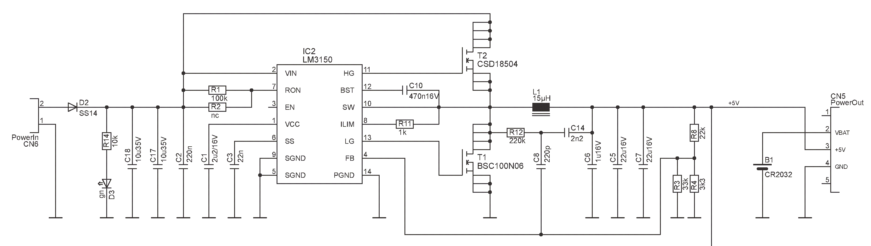
The design is rated 24 V (20-28 V) input to 5 V / 2 A output and was calculated using Webench.
Last year we produced several hundreds of this unit. Each unit was tested prior to shipment to
our customer. Now we got several boards back with defect power supply, and they all share the same
symptoms: The external high-side FET (CSD18504) has a short, and so connects the 24 V input voltage
directly to the regulators output - which causes excessive damage at the connected IPC board.
All these units worked fine first, but then failed after many hours or days of operation - some suddenly
during operation, others at turn-on.
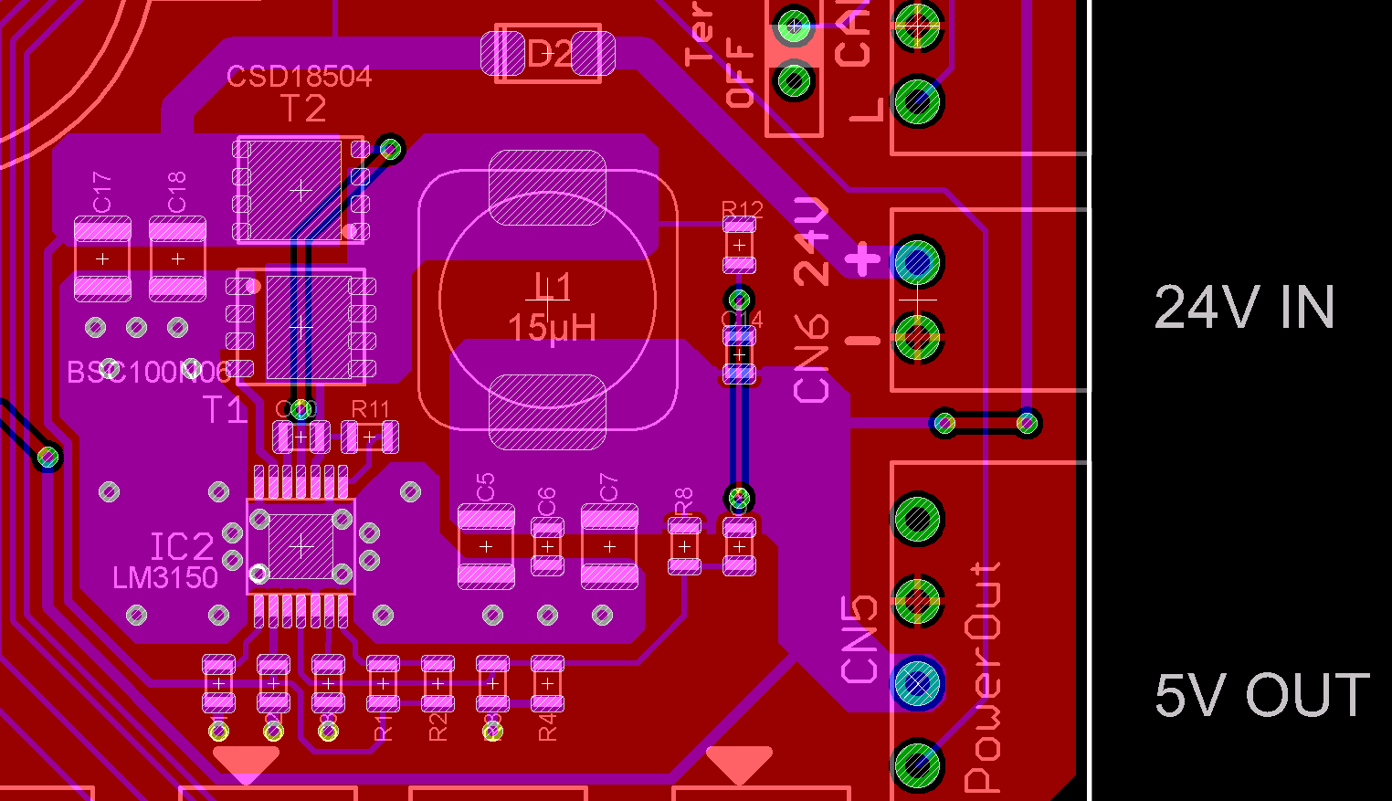
I didn't check yet if only the FET has died or if the controller chip also is defect now, to not delay this post. We are urgently looking for the cause of these failures, and hope that someone can help us with the analysis. I am attaching the schematic circuit and a pcb view from CAD that shows both layers and the components.   Many thanks in advance and best regards, Tilmann Reh
  • Hi Tilmann,

    Is the switching stable ? Can you please share the switch node waveform .

    Is their high ringing on the SW node ?

    Also in order to replicate the issue can you please turn on and off the input supply to the board and capture tthe inductor current with input and output viltage

    The Schematic looks mostly Ok to me with the exception of the ripple injection circuit . You would need to swap C8 and C14 .

    ---Ambreesh

  • Hello Ambreesh,


    yes, switching is stable and there is not much ringing.

    I am attaching a few scope screenshots showing some relevant curves.

    Unfortunately, I don't have a high frequency current probe, so I can't measure the startup currents in the inductor directly. However, from the timing and the voltages the inductor should never get into saturation (or even anywhere near), it is rated with 8 A (Würth 7447709150).

    The capacitors in the ripple injection feedback should be correct. They follow the Webench design and also work correctly in simulation and reality.

    Thanks & regards,

    Tilmann

    LM3150-measures.zip

  • Thanks Tilmann for sharing the waveforms .

    The Switching looks stable in the steady state .

    In the actual system , is there a long wire which is connected to the 24V input ? Where is the power source coming from ? Is there any other load connected to this 24V power source?Due to long wire harness inductance , you may see high voltage ringing and may be that is the cause of the damage . The solution would be to put some bulk capacitance just at the input of the board .

    Also if this is not cause by the input wire inductance , you may want to replicate the issue my turning on and off the input frequently and see the SW node waveform (since you dont have the current probes).There may also be a issue with Prebias startup ie the output cap may discharge during turn on and cause the damage . If that is the cause , you would see a voltage spike on SW node during the turn on process .

    Further as far as ripple injection circuit is concerned , the AC coupling cap should be 3 to 4 times larger than the integrator cap (RC cap across the inductor ) so that it wont change the FB calculation. Nevertheless if you are getting the stable switching and required output voltage setting , the ripple injection circuit should be OK and would not be cause of any failure .

    ---Ambreesh
  • Hello Ambreesh,

    thanks for your reply.

    In the target device, the supply is from a 24 V LiIon battery (that's why the regulator was calculated with 20-28 V input voltage). There's a wire of about 30 cm length from another board where the supply is switched with a high-side switch, and there (on that other board) also are two TVS  diodes (1.5SMC33A, one each before and after the HSS) to suppress any spikes that may come from the system (load changes etc.). Nothing else is connected to the output of the HSS or this wire, except for a step-down regulator that powers the logic and microcontroller on the other board.

    Can you be a little bit more precise/detailed about the "prebias startup" situation? I don't see how the output cap could discharge during turn-on and how/why that might be dangerous for the high-side FET.

    Tilmann

  • Hi Tilmann,

    You have a long wire connection to the board without sufficient capacitance . Also you have used ceramic capacitances (C17 and C18) which at DC bias of 24V  would offer much smaller capacitance then the rated 10uF . May be this is not the cause of failure but is definitely a weakness in the design . Please add 47uF/50V bulk capacitance at the input just near CN6 connector .

    Further , alternative solution can be to use the TVS , reverse protection as well as bulk cap on the same power board as mentioned above.

    Also during the PreBias startup, where the output cap is charged and the device is enabled, LOW side FET is turned on and current could flow in the reverse direction back through inductor and the Low Side FET back to input  .This excessive reverse current may cause the damage in Low side FET .

    ----Ambreesh

  • Hello Ambreesh, thanks for your comments.
    While it's not possible to move the HSS on to this board, we will do some tests with additional TVS and bulk caps. Tomorrow, I will be at the customers facility to do some measurements in the real environment.
    I think the PreBias situation is not our problem here, since the low-side FET never died.
    Thanks, Tilmann
  • Hello Ambreesh, I just returned from making measurements at the customer's location.

    To make it short: there's absolutely nothing critical with the input voltage in any state of operation. I am attaching a few screenshots showing the voltage at power on (rising very slowly with absolutely no ringing) and during the movement of a motor that is acting rather quickly, you can see the backlash caused be the motor speed regulator but it's still far from critical. No other load has even a measurable influence on the supply voltage.

    To make it even worse, I also got the information that by far the most of the defect units died while just staying powered on for some time, without doing anything. No power-on (or -off), no motor movements, no load changes. They just startet the devices and did some tests (without problems), then left them alone - and when coming back some time (maybe hours) later, the board would have died.

    I'm really at a lack of ideas right now...

    Thanks, Tilmann

    Power-Measures.zip

  • Hi Tilmann,

    This is very strange . When you say that the cusotmer is seeing the failure with no motor movement , what is the load connected to 5V output .Is it possible for you to probe SW node waveform at the cusotmer set up ? May be there is some issue  caused by cutomer's set up .

    Also with the motor running , i can see the boosted input voltage which indicates to the negative current following back to the battery .

    May i know where is this motor placed ? Is it working on 24V bus with the controller powered with 5V rail ?

    One thing you should do is to check the SW node and inductor current of the buck design when the motor is running . Is their any instability in the design when motor runs?

    The issue with the inductive load connected to battery is when the supply is disconnected , you could  see a negative going pulse on the input of the DC/DC converter which might damage the design .

    .

    ---Ambreesh

  • Hello Ambreesh,

    yes, it's strange - if it wasn't, I wouldn't have asked here... :-)

    The only load connected to the 5V output is the IPC board. The SW waveform is contained in the first zip (I did these measures with a real board). The current consumption of the IPC board is unlikely to change significantly, since all external I/O is connected via interfaces (mainly CAN). The ripple at the 5 V output is about 10-20 mVpp in operation, there also are only very small spikes at the input when the regulator is switching.

    The voltage from the battery is fed through a main power switch, after that all 24 V loads are connected, inclusing the other board that contains the HSS which finally switches the logic supply. The motors are intelligent drives that connect only to that 24 V rail (via an additional safety relay) and are controlled via CAN interface.

    For taking measurements at SW when that motor is running I would need to visit the customer again... However, remember that the failures happened when no motor was running (and nothing else was happening). We also are not talking about someone turning off the main switch exactly in that very moment when the motor is running or braking. (If that happens, the two strong TVS diodes on the other board will provide at least some kind of protection to our regulator here, and we also have a diode for reverse polarity protection right at its input.)

    Best regards, Tilmann

  • Hello Ambreesh,

    just for the record: I can now confirm that only the high-side FET is damaged. I exchanged it on four boards and they all work perfectly fine after that (except for the other parts that have been damaged by overvoltage on the 5 V supply...).

    Best regards, Tilmann

  • Hi Tilmann,

    Is the failure easier to replicate at the cusotmer place ? If that is the case , is it possible to replace the 40V FET with 60V same footprint FET and evaluate the board .

    ---Ambreesh

  • Hello Ambreesh,


    one problem is that we can't reproduce the failure at all. Since (until now) the failures appeared after a longer time of perfect operation and while nothing else happened, it is hard to observe as well. We were not able yet to force a failure within a real machine at the customers location.

    Of course I am already replacing the 40 V FET by a 60 V type (CSD18537) when repairing boards, to gain some more safety margin regarding the input voltage. However it's not practicable to replace all FETs in the 900 units we already delivered - particularly since we don't know what really caused the failure. Note that many of these boards are already assembled into machines, which are already delivered - or packed for delivery - to their final destination.

    OTOH, we also can't ignore these failures and simply deliver the machines, since we don't know if they may fail in the field later. :-(


    Best regards, Tilmann

  • Hi Tilmann,

    I also support the LM3150, and I've been following this discussion.

    I looked at the scope shots you sent (SDS00004 Motor Run.png in particular), and it is clear that there is some backfeeding of power from the motor driver into the 5V supply and then back into the VBUS of the LM3150. In the schematic you have above, there is a diode D2 that looks like it prevents any backfeeding of power from the LM3150 VBUS back into its supply. There does not appear to be anything clamping the VBUS.

    My feeling is that when the motor is turned off, the motor driver is injecting more power back into the VOUT of the LM3150, and there is even more power flowing back into VBUS. The scope shot you sent looks like it was taken during startup or running of the motor, I would suggest looking at the VBUS when the motor is turned off or stopping to get a sense of how VBUS is behaving.

    Regardless, it does look there should be some VBUS clamping with a TVS or other overvoltage protection device after the diode D2.

    Perry
  • Hello Perry,

    thanks for your reply - however I'm afraid that you didn't get the whole picture completely and right, so unfortunately your answers also don't match the situation. For clarification, I am attaching a sketch of the complete power supply system. Please also carefully read the whole thread again, since many details were already mentioned before.

    Please note that nothing but the IPC (a small single board computer) is connected to the 5 V output of this switching regulator. All the motors are intelligent drives that are directly connected to the 24 V supply rail. Between that rail and the input of this regulator, a high-side switch is located - with fat TVS diodes at both input and output which clamp any spikes that are injected on that 24 V rail.

    So there's definitely no backfeeding from any motor (or anything else) to the 5 V line, and also not backwards through the regulator to its input.

    The voltage curves of that screenshot SDS00004 are the result of the running drive's backfeed into the 24 V supply rail. From the viewpoint of this regulator, it is coming from external. Since that motor acts fast and short, such backlash is to be expected - however it's nowhere near critical; take care of the scale, the signal is within the range 25..28 V. The screenshot shows the braking and stopping of the motor, we triggered on the rising voltage of the supply rail. I confess that we missed to take a screenshot of the complete movement as well. (There also are other drives, but since these act slower and smoother, we could not detect any backlash from them.)

    Also please note that most of the failures occured in standby, with all motors stopped and nothing else happening.

    Regards, Tilmann

    PowerSupply.pdf

  • Hi Tilmann,

    Your right, I did not understand your system.  Based on your block diagram, I agree it does seem unlikely that the motors would backfeed so much that it would override the TVS protection and overvoltage the LM3150 board.

    Based on your description, the failure of the high-side FET does sound more like an overvoltage failure than an overcurrent failure. Did you ever observe the HS FET gate drive and the LS FET gate drive?  It might be good to check that there is not excessive ringing on those nodes.  I saw that you the switch node waveforms looked clean, but it is possible that the gate drives are ringing and causing issues in some rare cases. 

    I am puzzled by this as well.  I don't recall hearing about failures like this related to this part before. 

    Perry

  • Hello Perry,

    thanks for your reply. During development, of course we also checked the gate drive signals. They were perfectly fine - as expected; and what could cause any harm here? It's the straight implementation of the circuit and layout rules following data sheet and webench...

    Since we apparently don't get closer to the failure cause, we are now just observing if more of these boards would fail. (For repairs, we use the CSD18537, just to make sure we're on the safe side... and we also add one more TVS diode right at the input (at C17).)

    Regards, TIlmann