


Hi,
can you review below topic and comment of the six questions at the end of the thread?
We are developing a new board with Keystone2 processor. Attached to the EMIF16 of the Keystone2 processor there are several analog and digital
input and output devices. To reach our system performance requirements the read and write accesses to these devices must have a very short latency.
That means that the duration of read and write accesses must be as short as possible. Since the accesses on the EMIF are mostly random or
read-modify-write, we cannot use burst transfers by using DMA. Additionally some of our digital I/O devices need to use the wait signal.
In the past we made EMIF16 performance measurements on the K2EVM-HK development board with the XTCI6638K2KXAAW processor.
We observed the following EMIF performance (16 bit read) values with enabled extended wait mode:
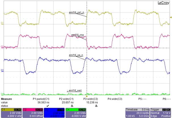
Length of Chip Enable (CE) low pulse: ~26 ns
Distance between risig edge of CE and falling edge of next CE access: ~30 ns
ð Access duration = ~56ns
Note: On the evaluation board we made measurements on the expansion header without a device on slave side.
The wait signal was hard wired on the expansion header to be inactive. Clocking: SYSCLK1 = 1167,36 MHz, ARMCPUCLK = 1375 MHz.
We used Linux-3.8.4-g42865b7. The test application only generates accesses to the EMIF Interface in a loop.
Based on this results we decided to use the Keystone2 processor for the new board design. We decided to use the AM5K2E04XABDA4, because we only
need the ARM cores, the DSPs are not necessary.
Now we are investigating the performance of the EMIF on our board and we are seeing that it is much below the results we reached with the development board.

Length of CE low pulse: ~22 ns
Distance between risig edge of CE and falling edge of next CE access: ~111 ns
ð Access duration = 133ns
Note: On our board we made measurements with the same conditions like in the past with the evaluation board.
The slave device on EMIF16 bus is a FPGA that acknowledges the access immediately. The wait signal is always inactive.
Clocking: SYSCLK1 = ARMCPUCLK = 1400 MHz.
We use RT-Linux. The test application only generates accesses to EMIF Interface in a loop.
We are wondering, if there are differences between the two processors, or if it is a problem of our register settings?
Following you will find the EMIF register settings we used on both processors:
EMIF Settings on the development Board:
RCSR= 0x40000205
AWCCR= 0xf0040080 (WP1=1, WP0=1, CS5_WAIT=0, CS4_WAIT=0, CS3_WAIT=1, CS2_WAIT=0, MAX_EXT_WAIT=128)
A1CR= 0x04422218
A2CR= 0x40100081 (SS=0, EW=1, W_SETUP=0, W_STROBE=1, W_HOLD=0, R_SETUP=0, R_STROBE=1, R_HOLD=0, TA=0, ASIZE=1)
A3CR= 0x00000000
A4CR= 0x00000000
IRR= 0x0000000C
IMR= 0x00000000
IMSR= 0x00000000
IMCR= 0x00000000
NANDFCR= 0x00000001
NANDFSR= 0x00000003
PMCR= 0xfefefefe
NFECCCS2= 0x00000000
NFECCCS3= 0x00000000
NFECCCS4= 0x00000000
NFECCCS5= 0x00000000
NANDF4BECCLR= 0x0000033f
NANDF4BECC1R= 0x00000000
NANDF4BECC2R= 0x00000000
NANDF4BECC3R= 0x00000000
NANDF4BECC4R= 0x00000000
NANDFEA1R= 0x00000000
NANDFEA2R= 0x00000000
NANDFEV1R= 0x00000000
NANDFEV2R= 0x00000000
EMIF Setting on our own Design:
RCSR= 0x40000205
AWCCR= 0xf0040080 (WP1=1 WP0=1 CS5_WAIT=0 CS4_WAIT=0 CS3_WAIT=1 CS2_WAIT=0 MAX_EXT_WAIT=128)
A1CR= 0x7ffffffd
A2CR= 0x40100081 (SS=0 EW=1 W_SETUP=0 W_STROBE=1 W_HOLD=0 R_SETUP=0 R_STROBE=1 R_HOLD=0 TA=0 ASIZE=1)
A3CR= 0x7ffffffd
A4CR= 0x7ffffffd
IRR= 0x0000000d
IMR= 0x00000000
IMSR= 0x00000000
IMCR= 0x00000000
NANDFCR= 0x00000000
NANDFSR= 0x00000000
PMCR= 0xfefefefe
NFECCCS2= 0x00000000
NFECCCS3= 0x00000000
NFECCCS4= 0x00000000
NFECCCS5= 0x00000000
NANDF4BECCLR= 0x00000000
NANDF4BECC1R= 0x00000000
NANDF4BECC2R= 0x00000000
NANDF4BECC3R= 0x00000000
NANDF4BECC4R= 0x00000000
NANDFEA1R= 0x00000000
NANDFEA2R= 0x00000000
NANDFEV1R= 0x00000000
NANDFEV2R= 0x00000000
Please can you give us some help, how to reach the EMIF performance of the development board on our own design?
Here are our detailed questions:
- As described above, the distance between the CE pulses is much longer on our new design than on the development board (30ns vs. 110ns). Do you have an explanation for this behavior? Can you help us to improve the values on our new design?
- We observed a different behavior between the four CE signals of the EMIF. CE0, CE1 and CE2 have an identical behavior, but on CE3 the write access duration (access start to next access start) is about 20ns shorter than on the other CE signals (79ns vs. 97ns). Can you confirm this behavior?
- Since we are using the “wait enabled mode”, we also investigated the “wait disabled mode”. On the development board the access duration decrease from 56ns to 46ns after disabling the wait mode. On our new design the access duration decrease from 140ns to 77ns after disabling the wait mode. Compared to the development board on our new design the wait mode obviously has a huge influence to the access duration. Do you have an explanation for this different behavior? How do we reach the values from the development board?
- We observed another unusual behavior in the “wait disabled mode”. If we increase the strobe length in the A2CR register the CE pulse length will be increased accordingly, but the distance between the CE pulses will be increased as well. We expect, that only the pulse length will be affected by the strobe setting in the A2CR register. Can you explain this behavior?
- In the “wait enabled mode” we additionally observed an unusual behavior. According to the datasheet the wait signal must be inactive for at least 2 cycles to complete an access. We observed, that neither 2 nor 3 or 4 inactive wait cycles were enough to complete a read access. In our case we need to hold the wait signal inactive until the read access is completed (until rising edge of OE). Not till then we can activate the wait signal again for the next read access, but we additionally have to add 3 hold cycles in the A2CR register to take care, that the next access even recognizes the wait signal. In our opinion this is a strange behavior compared to the documentation. Do we use the wait signal in a correct manner? Do you have any explanation for this behavior, or can you tell us how to avoid it?
- One last question according the PLL: According to Figure 4-1 on page 14 of the datasheet the quad core ARM A15 Version of the Keystone2 (that we are using: AM5K2E04XABDA4) should have a Main PLL and an ARM PLL. But in the further description an ARM PLL is not mentioned any more. It seems, that the quad core has only a Main PLL like the dual core (see Figure 4-2 on page 15). Is that correct

