I'm trying to debug a problem with the TMP007 sensor on a CC2650 SensorTag. The sample code provided for the SensorTag can't access the TMP007, which fails to acknowledge its I2C address. The same firmware appears to work fine for other people, so I'm wondering whether the TMP007 on my SensorTag could be damaged or incorrectly installed.
I've read the TMP007 datasheet and app note AN-1112 DSBGA Wafer Level Chip Scale Package (Rev. AG), which covers WLCSP packages in general. Unfortunately I haven't found the information I'm looking for.
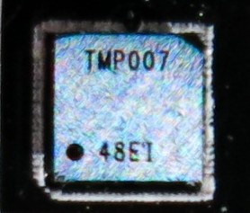
Here's a photograph of the chip on my SensorTag:
First of all, is the circular dot at the lower left marking the location of pad A1 (on the underside)? Do the pads then continue A1, A2, A3 moving to the right and A1, B1, C1 moving up the image?
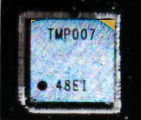
Second, is the package expected to be perfectly square with no corners missing? Here's another picture highlighting what appears to be damage to the upper two corners of the package:
I'm not sure whether the missing corner at the top right is deliberately cut off to indicate orientation, cosmetic damage during manufacturing or damage that could cause product failure.


