


The increasing performance demands of smartphones and tablets combined with the need to fit more functionality in the same space dictate a requirement for denser power supplies in these end equipments. Higher currents must fit into smaller IC packages. Higher switching frequencies are used to shrink the capacitor and inductor sizes, decreasing the total solution size. But with all of this shrinking comes a tremendous increase in the power density. There’s more power (and thus more Watts of loss) in a smaller space. This requires a keen eye on the thermal design of the solution as well as the power supply ICs themselves.
Focusing on an example power supply IC in such a system, consider the thermal challenge at hand: it must convert a lithium-ion battery voltage (3.6V nominal) to a regulated 1.2-V output voltage that supplies 3A. And then it must find a way to get rid of the energy lost in the process! Even at 85+% efficiency (which is pretty good for a tiny power supply switching at 3+ MHz), this is about 0.6W of loss that must exit the power supply.
Where does this power go? Eventually, it must go into the surrounding ambient environment (the air) after creating a temperature rise across the thermal impedance of the power supply to the air. If this temperature rise is too high (because the thermal impedance or power loss are too high), the power supply might burn your finger when touched (ouch!) or even reach its thermal shutdown temperature (ouch for your system!).
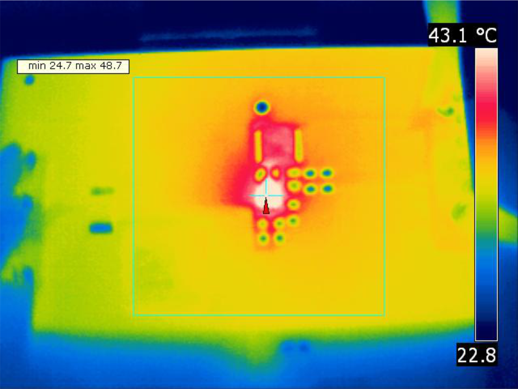
Thermal image of the TPS62085 buck-converter in new HotRod package (Vin=6V, Load=3A)
What is the system designer to do? The answer is simple to explain but difficult to implement: he or she must design a low enough thermal impedance to not cause too high of a temperature rise while keeping the solution size small. A good starting point for calculating the temperature rise is the ΘJA of the power supply IC. When multiplied by the power dissipation, this computes the temperature rise of the device. Now, can we find a power supply that has a low enough thermal impedance as well as a small enough size?
Yes we can! Through various power supply IC packaging options, the tradeoff of size to ΘJA can be made by the designer. If smallest size is most important, then consider the 2mm x 2mm TPS62360 in a chipscale package. If its ΘJA of 94.8 °C/W is too high for a given application, then consider the slightly larger TPS62090. At 3mm x 3mm, this QFN package is large enough to contain an exposed thermal pad which gets the ΘJA down to a low 47 °C/W. Is 3mm x 3mm too large? Then, try the TPS62085 which boasts a ΘJA of 69.8 °C/W in a 2mm x 2mm QFN package. I am sure that you can use one of these options to get the heat out of your power supply IC.
How are you cramming more and more functionality into a smaller size in your designs?
Additional Resources:
- TPS62085EVM-169 3-A step-down converter evaluation module
