Electronics such as smartphones, tablets, notebooks and wearable products are becoming more multifunctional, smaller and slimmer. Achieving higher functionality in smaller form factors requires extremely tiny ICs. Many times, different package types help reduce size and solve various design challenges. Take operational amplifiers (op amps), for example; wafer chip-scale packages (WCSP) typically enable the smallest possible footprint for optical modules and wearables, while flat no-lead packages such as quad flat no-lead (QFN) or dual flat no-lead (DFN) inspire differentiated audio functionality in personal electronics where small size, high performance, and easy testing and tuning are essential. Small-outline transistor (SOT) packages like SOT553 are suitable for emerging industrial applications such as field transmitters, which require a wide supply but a small footprint in a user-friendly leaded package.
The rapid evolution of mobile devices is driving package technology innovations, but the smallest possible package will always be the size of the die itself. The WCSP is a type of package that can be almost as small as the die, so it’s desirable in applications like medical diagnostics, fitness monitoring and handheld electronic devices. The OPA2376 in WCSP (1.11mm by 2.15mm by 0.625mm) is a device commonly used for signal conditioning purpose in the areas mentioned above.
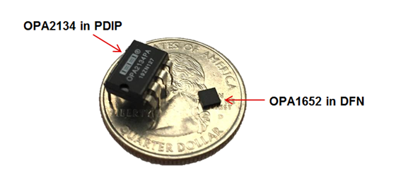
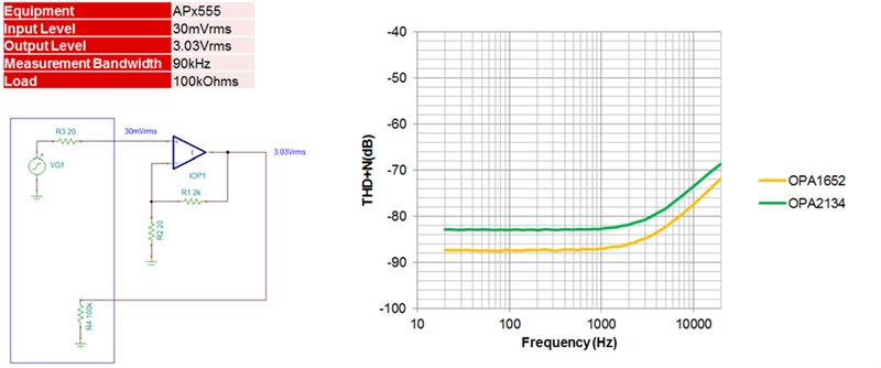
Audio in portable devices is another example where tiny packages are inspired by the consumer needs. Traditionally in the professional audio world, audiophiles like to use op amps in the dual inline package (DIP), which is more DIY-friendly for audio designers. The OPA2134 from the legacy Burr-BrownTM audio portfolio, is such an example with great audio reputation. However, with the increased demand of high-quality audio in portable devices, tiny-package high-performance audio ICs are required in order to enable the high-fidelity sound in a space-constraint design. With the implementation of the DFN package on the OPA1652 (Figure 1), a performance upgrade to the OPA2134, you will find a high-performance current-to-voltage converter with great sound quality for cost-optimized portable audio equipment, smartphones and gaming motherboards. Figure 2 shows the total harmonics distortion and noise (THD+N) performance of the OPA1652 and OPA2134 with common-mode impedance mismatching.
Figure 1: OPA1652 (DFN) versus OPA2134 (PDIP)
Figure 2: THD+N test in a gain of 100: the OPA1652 vs. the OPA2134
A tiny package may not be the only consideration for wearable devices. These types of applications typically spend most of their time in sleep mode until they are needed to measure biometric data. This requirement has inspired op amps with a shutdown feature in tiny QFN packages. For applications where power consumption is a vital concern, tiny packaging helps enable product innovation, because you can achieve both low power and a small form factor. The OPA2316S in a X2QFN (1.5mm by 2mm by 0.4mm) operates down to 1.8V with a wide bandwidth of 10MHz, as well as rail-to-rail performance, making it suitable for battery-powered designs.
Some industrial factory automation applications also require a tiny package. Often, designers prefer devices with small-outline lead packages that are easy to prototype, layout and swap with pin-to-pin-compatible ICs. The OPA171 is one of the first micropower 36V op amps offered in both a single SOT553 (1.6mm x 1.6 mm) package and a dual, very-thin shrink small outline package (VSSOP) (2.0mm x 3.1mm), providing an optimized combination of low cost and performance for applications such as tracking amplifiers in power modules, transducer amplifiers and battery-powered instruments.As a fundamental building block for a signal chain, op amps must keep pace with the emerging electronic design trends. TI has developed products in some of the smallest packages available, including WCSP, QFN/DFN and SOT553. With innovations in design and technologies, more tiny-package, low-power precision op amps are on the way. Browse TI’s tiny op amp portfolio to find the best one for your next project.
Additional resources
- Read the Analog Applications Journal article, “Distortion and source impedance in JFET-input op amps.”
- Learn more about the TI Design, “A High-Fidelity Headphone Amplifier for Current Output Audio DACs Reference Design”
- Visit the “Headphone Amplifier for Voltage-Output Audio DACs Reference Design”


