

In my last blog post, I discussed why instrumentation amplifier power supply rejection ratio (PSRR) and common mode rejection ratio (CMRR) improve as the amplifier’s gain increases.
Returning to the simplified model of an instrumentation amplifier shown in Figure 1, we recall that PSRR and CMRR are input referred specifications.
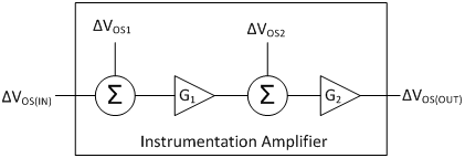
Figure 1: A conceptual model of an instrumentation amplifier
In higher gains, the shift in the second stage offset is divided by the gain of the input stage when it is referred to the input:
Here is where the conceptual model of the two stage amplifier is somewhat incomplete. For example: what if the changes in offset of the two stages are equal and of the same polarity? That is to say:
Comparing the improvement in PSRR for an amplifier in a gain of 1000 vs. a gain of 1:
The input referred offset shift is cut in half, which is a 6 dB improvement in PSRR. But the PSRR of a typical instrumentation amplifier may improve by up to 30 dB when increasing the gain from 1 to 1000. Clearly, ΔVOS1 must be much less than ΔVOS2 to account for this level of improvement.
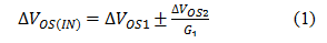
A closer look at the internal structure of a 3 op-amp instrumentation amplifier in Figure 2 reveals how this is possible. The output stage, consisting of amplifier A3 and resistors R3, R4, R5, R6, is configured as a difference amplifier. If the resistors R3, R4, R5, and R6 obey the ratio:
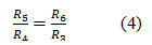
Then the output stage will amplify only the differential voltage from the input stage and reject any voltages common to both inputs.

Figure 2: The standard topology of a 3 op-amp instrumentation amplifier
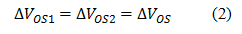
The input stage of the amplifier consists of two amplifiers: A1 and A2. A change in the power supply voltage or common-mode voltage produces a corresponding shift in the input offsets of these two amplifiers, shown in Figure 3 as ΔVOS1A and ΔVOS1B.

Figure 3: The input stage amplifiers of an instrumentation amplifier with their individual offsets
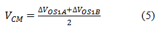
Let’s consider the case where the non-inverting inputs of A1 and A2 are grounded, and the input stage is configured for a gain of 1. Now, assume a change in the power supply voltage causes a shift in the input offset voltages of A1 and A2. The output of each amplifier with respect to ground will mirror this shift in offset voltage. The output common-mode voltage of the input stage will be:
And the output differential voltage will be:
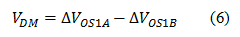
Recall that the output stage difference amplifier rejects common-mode voltages; only the differential voltage is passed to the output. Therefore, the input referred offset shift of the input stage (ΔVOS1) is actually determined by the DIFFERENCE between ΔVOS1A and ΔVOS1B and not their absolute magnitudes!
With careful IC design and layout practices, these two offsets are matched fairly well, reducing the input stage offset shifts to about a tenth of the output stage on average.
The CMRR and PSRR specifications of an instrumentation amplifier don’t magically improve with increasing gain. It is really the result of the multi-stage topology and difference amplifier output stage.
Careful matching of the input amplifiers and trimming of the output stage resistors allows modern IC instrumentation amplifiers to provide electrical engineers with the huge amount of rejection that we’ve become accustomed to.


