

Many applications, such as motor drives and power inverters, require isolated measurements of both current and voltage. Although optimized for current sensing applications, TI’s isolated delta-sigma modulators enable high-performance voltage measurements.
If you are designing such applications, there are important details to remember when choosing the resistor divider.
For example, assume one needs to monitor the input voltage to a power inverter. Let’s suppose the maximum input voltage to the inverter is 390 VAC and that a delta-sigma modulator with +/- 250 mV linear input range (such as the AMC1304 or AMC1305) is used.
The first inclination to carry out the voltage sensing is to implement the circuit shown in Figure 1.
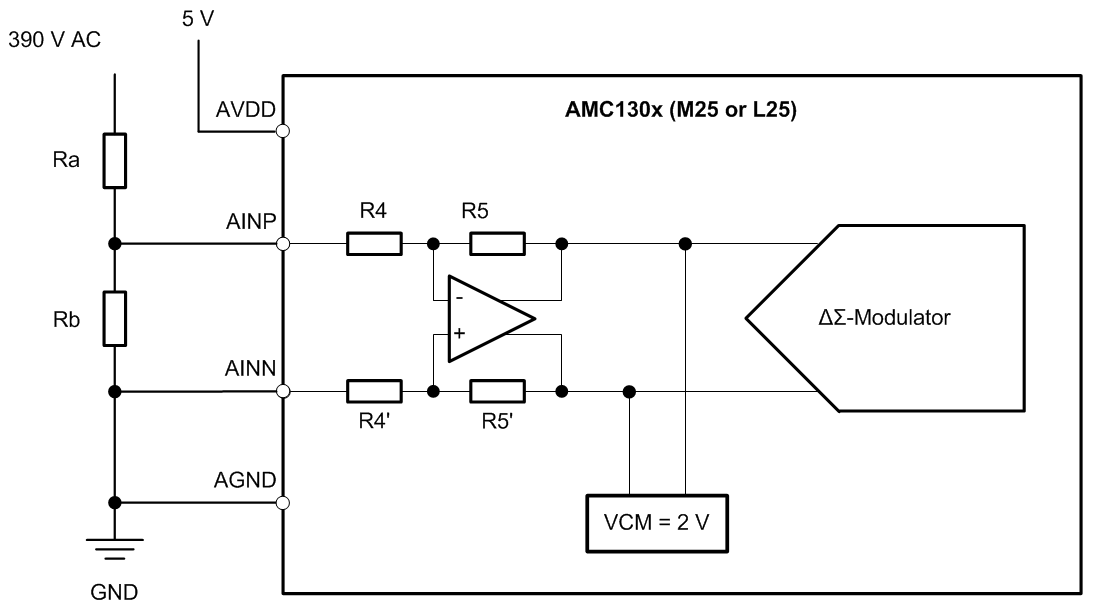
Figure 1: First rough solution to perform isolated voltage monitoring
The resistor divider formed by Ra and Rb in Figure 1 is governed by Equation 1.
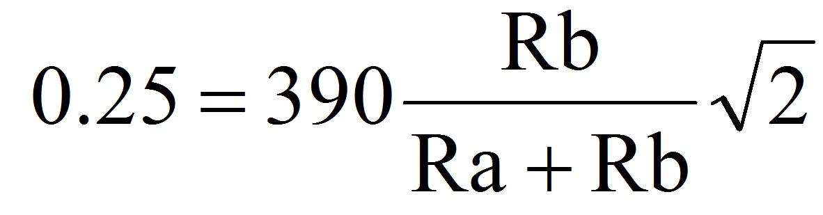
Equation 1
Note that the voltage drop across Rb has been set to 0.25 V in order to efficiently use the available linear input range of the delta-sigma modulator.
Suppose that one of the design requirements is to limit the power dissipation in the Ra + Rb series combination to less than 70 mW. This power dissipation and Equation 1 yield the values of Ra = 4.4 MΩ, Rb = 2 kΩ and a peak voltage drop of 250.59 mV across Rb. This voltage drop is close enough to the desired linear input range target and the resistor values are standard.
Upon simulating the circuit in Figure 1, designers may find an unexpected result. The voltage drop across Rb (shown in Figure 2) has about 58.4 mV of offset. Further, instead of reporting 500 mVpp, the simulator reports 457.3 mVpp. Given that the input has no DC component, one would expect to observe no offset in the differential input.

Figure 2: Simulated differential input
The reason behind the mismatch between calculated and simulated data becomes clear upon carefully reviewing the delta-sigma modulator datasheet: The input structure of AMC1304’s and AMC1305’s devices has an input bias current that should be taken into account when performing measurements using large shunts. Moreover, this input bias current depends on the input signal and causes more than a mere input signal offset. See Figure 54 as an example in the AMC1305 datasheet.
For the circuit in Figure 1, the value of Rb is more than a negligible fraction of the differential input impedance of the AMC1304 and AMC1305 devices. Following the recommendations in the datasheet, one can refine the voltage sensing circuit and better predict the deviation of the input differential signal from the theoretical value expected when using the resistor divider equation.
Figure 3 shows the refined voltage sensing circuit. Note the following changes:
a) Ra was split into two (R1 and R2) in order to maintain the proper creepage and clearance requirements based on the large voltage drop in these resistors.
b) A new resistor (R3’) was added in order to eliminate the offset observed in the circuit depicted in Figure 1.

Figure 3: Refined voltage monitoring circuit
In essence, what happens in the circuit depicted in Figure 3 is that the signal-dependent input bias current IIBN, when flowing through R3’, compensates the offset previously observed at the cost of a mismatch in the input resistance connected to the AINP and AINN terminals of the delta-sigma modulator.
As explained in the AMC1304 and AMC1305 datasheets, there is an expected difference between the resulting differential input voltage (AINP – AINN) and the theoretical voltage drop on R3 given by the resistor divider equation. Such discrepancy can be expressed as a gain error, as shown in Equation 2.

Equation 2
Figure 4 shows the simulation result for the refined voltage sensing circuit. Note that the prediction in Equation 2 matches reasonably well the simulated result as shown in Equation 3.
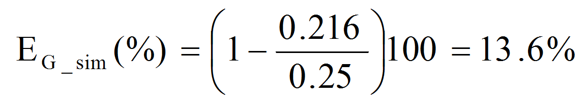
Equation 3

Figure 4: Simulation result for refined circuit
In order to obtain an input closer to +/-250 mV, the value of R3 and R3’ need to be increased. For example, setting R3 = R3’ = 2.38 kΩ provides a peak input of 250.5 mV. Note, however, that system calibration will be required since the tolerance in R1, R2, R3, and R3’ will most likely be higher than the accuracy requirements of most applications. At the end of the day, whether to use the original resistor values shown in Figure 3 or modify them to maximize the input voltage to the delta-sigma modulator is the designer’s choice.
Additional resources:
Learn more about AMC1304 and AMC1305, delta-sigma modulators with reinforced isolation.
Click here to get information on the isolated current shunt and voltage feedback reference design (TIDA-00171)
See more posts in our delta-sigma ADC basics series.
