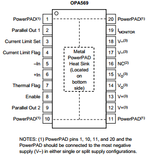
The PowerPad™ is a great package feature that allows operational amplifiers and other linear circuits to deliver otherwise unattainable output power from a device packaged in a small outline (SO) package. The PowerPad™ provides a highly conductive thermal path from the back of the integrated circuit die to an external heat sink, or to a copper PC board plane acting like one. The product datasheet is specific about the electrical potential the PowerPad™ must be connected to, which is usually the most negative supply level. That is 0 V, or ground, for an operational amplifier using a single-supply or V- for one using dual supplies (V+ and V-).
An example from the OPA569 power operational amplifier datasheet is shown below. Note Figure 1 specifies that the PowerPad™ should be connected to V-. In reality, it can’t be connected to a voltage more positive than V- without potential issues. The V- power pin and the PowerPad™ are hardwired together. Some high power operational amplifiers such as the OPA548 packaged in a TO-220 package have a similar connection requirement for its metal tab.
Figure 1
If the pad or tab isn’t connected to the correct potential, which is the most common problem, the amplifier may be thrown into a completely different realm of DC operating conditions that can lead to abnormal operation, excessive heat generation or even damage. Other amplifiers may exhibit less dramatic effects such as altered DC and AC performances.
Analog integrated circuits (ICs) are comprised of many different transistor, resistor and capacitor structures. Each structure must coexist with the others and are usually electrically isolated from each other. This is most often accomplished in ICs by junction isolation and to a lesser extent using dielectric isolation. Implementation varies by process. Figures 2A and 3 illustrate the basic isolation structures.
Figure 2A shows a cross-section of two NPN bipolar transistors residing adjacent to each other. Their collector, base and emitter regions are shown. A P-region that connects down to the P-substrate resides between the two collectors. The N-collector, in conjunction with the adjacent P-region, creates a diode. The P-regions between the transistors connect to the P-substrate which is attached by an electrical and thermally conductive medium to the SO package PowerPadTM or the TO-220 package tab.
Figure 2A: Junction isolated NPN pair cross-section Figure 2B: Vertical PNP cross-section
If the diode anodes are biased at the most negative voltage, and the other transistor regions are biased more positive, the diodes are reverse biased, preventing current flow between the transistors. They are electrically isolated.
Another structure where the die must be at the most negative voltage is the vertical PNP transistor shown in Figure 2B. The transistor collector is the actual P-substrate region. This transistor structure is commonly used as the PNP emitter follower in a complementary NPN-PNP op-amp output stage.
High performance analog ICs also may use dielectric isolation where the electrical components reside and are isolated within non-conductive tubs. Figure 3 shows a cross-section for a similar NPN pair. The transistor structures have a thin layer of insulating silicon dioxide (SiO2) between them and the polysilicon tubs. Dielectric isolation is used for both bipolar and MOS based circuits.
Figure 3: Cross-section of dielectrically isolated NPN transistor pair
Since the transistors are isolated by insulation, one may question why the tying the P-substrate to V- would be necessary? Electrically, there isn’t a concern about shorting two different potentials together. It comes down to the transistor DC and AC characteristics, and circuit’s design is established with the substrate at the V- potential. Electrical characteristics such as the capacitances shown in Figure 3 are defined and incorporated into the circuit design under that condition. Biasing the substrate at a different potential may alter the amplifier’s AC bandwidth, transient response and/or distortion performances.
If a datasheet indicates that the PowerPad™ is internally connected to V- but doesn’t say much more, connect it to the V- PC board plane. This ensures the amplifier’s V- pin and the PowerPad™ will be at the same potential. Lastly, if the datasheet says the PowerPad™ must be soldered to the plane - do it! It assures not only good electrical and thermal connections between them but also adds structural integrity to the package itself.
Related resources:
PowerPadTM Thermally Enhanced Package, OPA569 data sheet (pages 18 -19)
Basic Integrated Circuit Engineering by Douglas Hamiltion and William Howard. McGraw-Hill, 1975.
(Click on images to enlarge.)


