

In the last few months, I’ve seen at least four cases of the wrong understanding of the “real Vos” of an op amp.
Figure 1 shows the specs for the OPA363 op amp, a single supply 1.8V to 5.5V op amp with 7MHz of unity gain bandwidth and a 5V/us slew rate. I’ve put a box around the real Vos of the OPA363 in the table below.
NOT! The real Vos of the OPA363 is directly dependent on how it is used in your application!
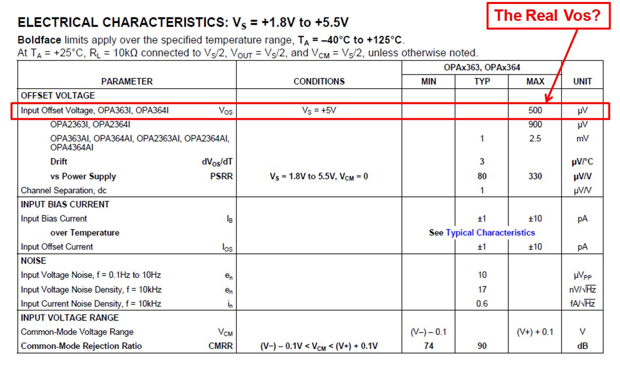
Figure 1
Let’s look at how to calculate the real Vos for your application and keep your designs meeting their specification.
The key contributors to DC Offset voltage are:
1) Vos_drift (Vos change with temperature)
2) Vos_PSRR (Vos due to power supply rejection ratio)
3) Vos_CMRR (Vos due to common mode rejection ratio)
4) Vos_initial (Vos under factory test conditions)
Each of these individual contributors to Vos can have a positive or negative magnitude. We’ll do our initial computation assuming they all have a positive polarity.
Figure 2 uses information from Figure 1 to compute the individual contributors of offset due to the end application. It’s important to decipher the factory test conditions for Vos_initial, as listed in Figure 2.
Vos_drift is calculated by using the temperature difference between 25C and the end application.
Vos_PSRR is computed by noting the difference between the supply used in the end application and the supply used for Vos_initial test.
Vos_CMRR requires a conversion of the CMRR specification, given in dB, to a linear attenuation specification given in uV/V.
Now we have all of the contributing factors to the real Vos based on our end application.
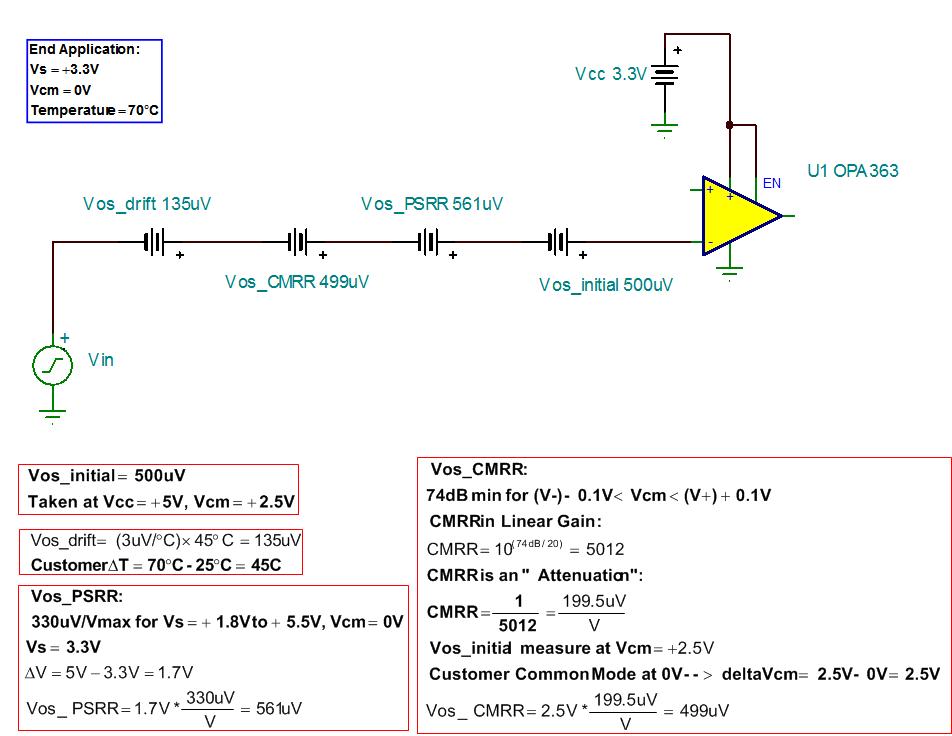
Figure 2
So now what do we do with the individual contributors to Vos?
All data sheet specs are usually obtained using a +/-3 sigma truncation of a typically Gaussian distribution of parts over process variations. So we can obtain the Vos_total _RSS by taking the root sum of squares of each individual contributor.
This RSS total implies a +/- 3 sigma coverage, or that 99.7% of all devices used in our application will be less than or equal to our computed Vos_total_RSS. This also means that 0.3% of parts can be larger than our Vos_total_RSS.
If we want a conservative design margin, we can add all of the errors to yield Vos_total_max.
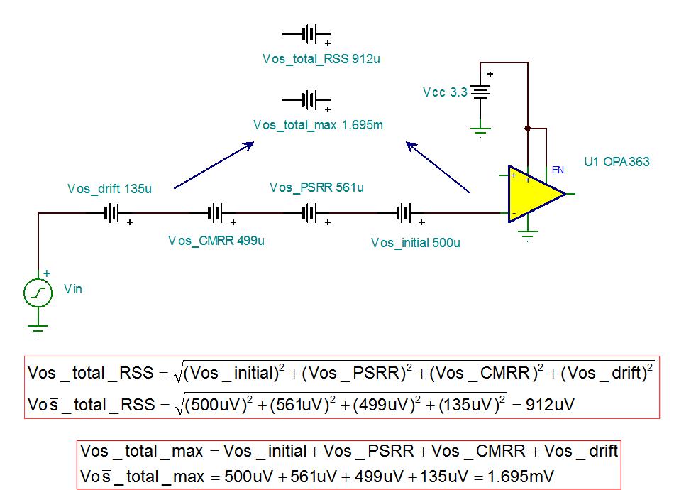
Figure 3
Figure 4 shows the summary of our real Vos investigation. Whether you decide to use Vos_total_RSS or Vos_total_max, remember that the totals can be positive or negative in polarity, as shown in Figure 4.
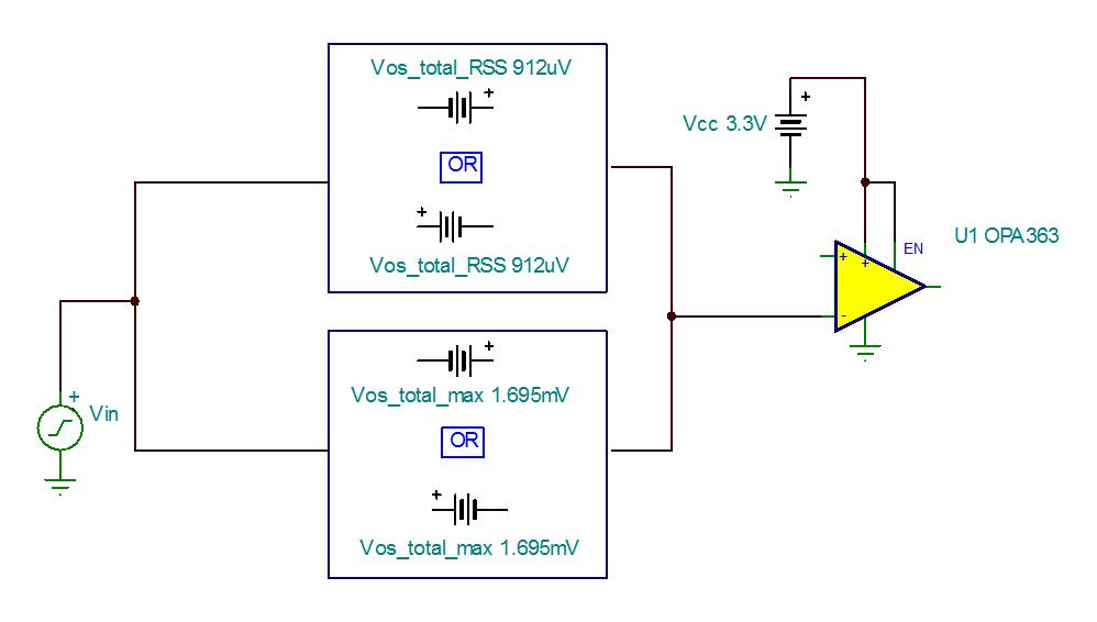
Figure 4
Hopefully, you’ll consider the real Vos in your next application and avoid any unwanted surprises when your product goes to production.
And if you want to learn more about statistics and op amp noise, you might want to check out the book written by my boss, Art Kay (Kay, A., Operational Amplifier Noise, Newnes, 2012).


