This thread has been locked.

If you have a related question, please click the "Ask a related question" button in the top right corner. The newly created question will be automatically linked to this question.

LMH32401: LMH32401: PCB design for this transimpedance amplifier

Part Number: LMH32401
Other Parts Discussed in Thread: OPA2182

Hi Team

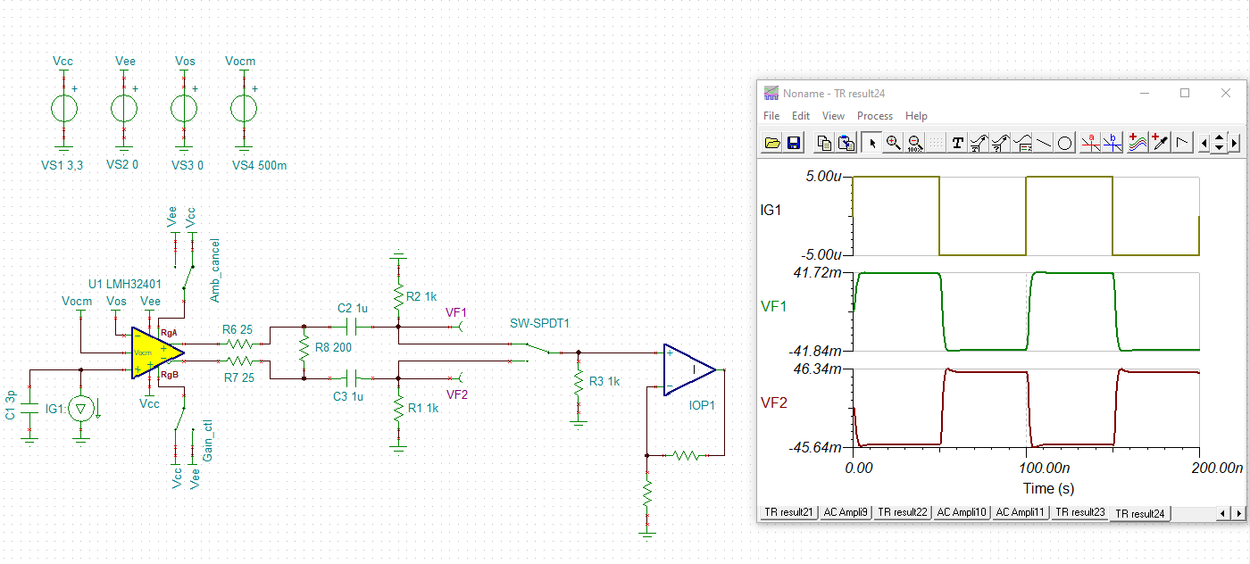
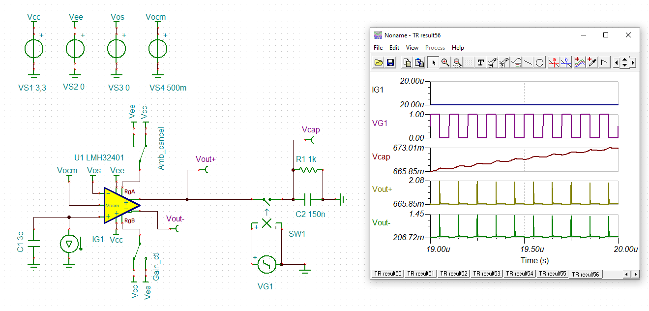
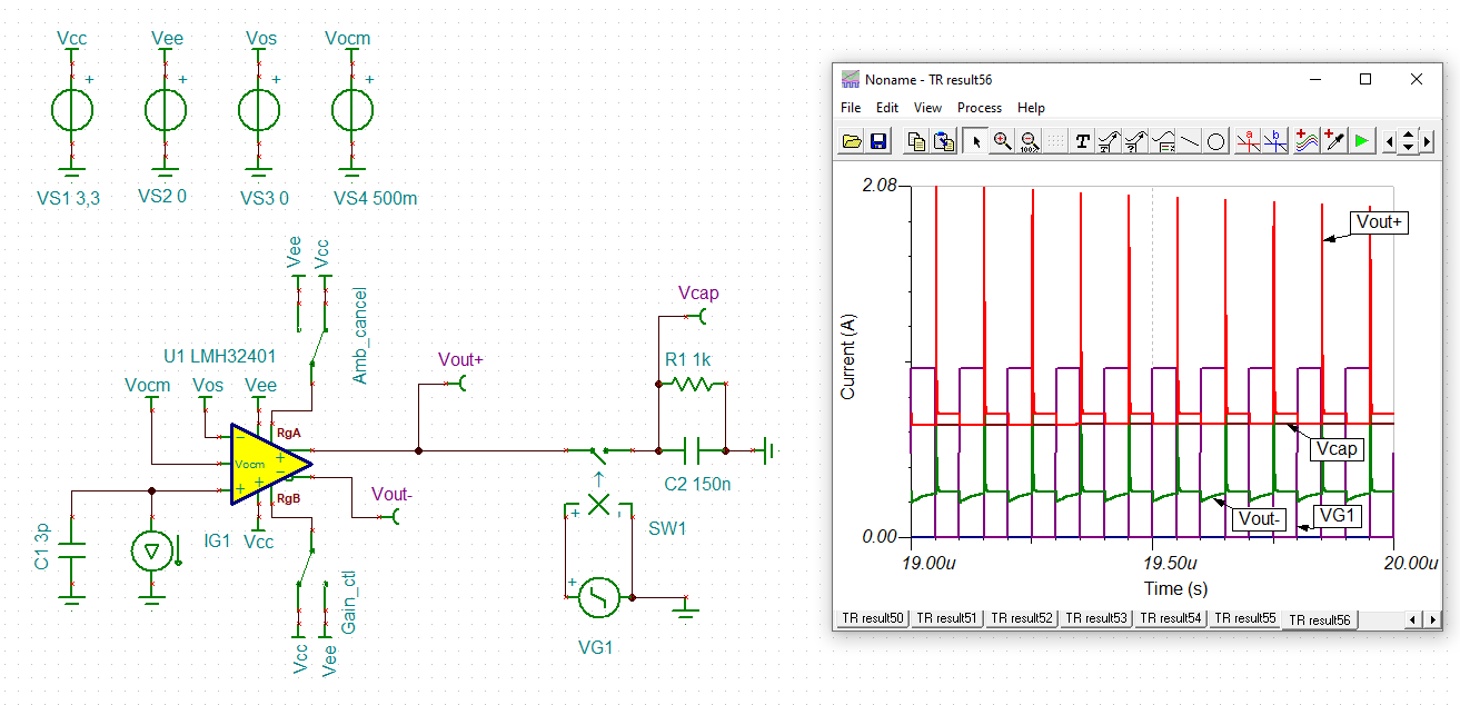
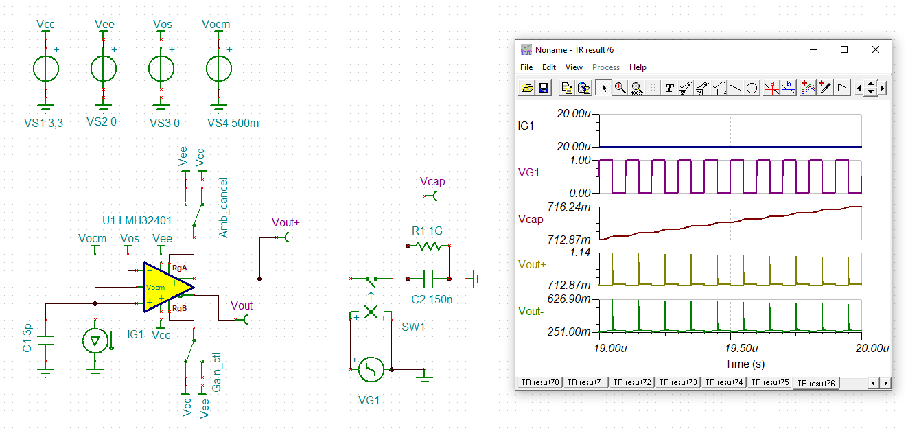
Hello, I am trying to have an analog front-end transimpedance amplifier for our sensor. When designing the PCB, the most common solution would be having a SMA socket on the broad then connecting the sensor with PCB using the sma cable. However, for this kind of high speed transimpedance amplifier, any addition capacitors on the input might cause instability problem. I know cables will introduce a lot of capacitance. Then what do you suggest to feed the input current? Should I have a sma socket on the pcb? Or what did you guys do when you test this chip and get all the data on the data sheet?

Thank you.

Best regards,

William

  • Hi William,

    if possible, I would make a direct connection. No socket and no cable. It's not only cable capacitance but also stray inductance which you should avoid at the input of TIA.

    Kai

  • Hi Kai

    Thank you for your reply. Then how about the output capacitor? Will this affect the stability and how much capacitor it can tolerate?

    Because we might have another voltage amplifier after the LMH32401. The capacitor between them is pretty large, as the schematic is shown below. Do you see any problem with this configuration?
    Thank you.
    Best regards,
    William
  • Hello William,

      I agree with Kai, a direct connection with the photodiode placed as close as possible to the input of the amplifiers is the best method to eliminate additional impedances. 

      In this type of setup, there shouldn't be any issue. Have they chosen a FET input amplifier that will follow the LMH32401? 

    Thank you,

    Sima

  • Hi Team
    Thank you for your reply. I am using OPA2182 after the LMH32401. I do not know OPA2182 is made of CMOS or BJT. I am wondering why you think this is important? 
    Also, how about the bandwidth? Will 150nF after the LMH32401 affect the BW of the LMH32401? Because the other side of 150nF capacitor is connected as AC ground. And the pole of 10ohm and 150nF is pretty small.

    Thank you.

    Best regards,

    William

  • Hi William,

    do you want to connect a differential amplifier to the output of LMH32401? In this case your differential amplifier should contain four (identical) resistors as shown in figure 11-1 of datasheet of OPA2182.

    Take care that the OPA2182 is much slower than the LMH32401. By this you can not maintain the high bandwidth of LMH32401. Is this desired?

    Can you tell something about your sensor signal, about its bandwidth?

    Kai 

  • Thank you for your reply. Sorry, I simplified the schematics a little bit in the earlier email. I have a single pole double throw switch in between. The switch is working at the frequency around 10MHz. So the output of the TIA will be demodulated at fin-10MHz (switch works as mixer).

     
    Our voltage amplifier does not have to be fully differential but has to be AC coupled. So I have to use an input capacitor and the gain is defined by the ratio of the input capacitor and the feedback capacitor. I do not think the structure on the datasheet of OPA2182 11-1 works for me.
    For the switch, when the switch is on, the resistance is 4ohm, which is pretty small. So in this case, it looks like the 150nF capacitor is directly connected to one of the outputs of TIA. Then on the other side of the 150nF cap, it is AC ground. So 10ohm+4ohm and 150nF generated a very low bandwidth low pass filter. So, when the capacitor is connected to one of the outputs of the TIA, in theory, that output will have a very large attenuation for the signal around 10MHz. I have several concerns regarding this very large 150nF capacitor.

    1. Will this capacitor affect the stability of the TIA when the capacitor is connected to one of the outputs of the TIA?

    2. When the capacitor is connected to one of the outputs, that output will have large attenuation. Will this affect the other output? You can see the simplified schematic below. When OUT+ is connected to 150nF, OUT+ will get a very small signal around 10MHz (gain is much less than 10kohm). How about OUT-? Is the gain at OUT- still 10Kohm? 
    Thank you.
    Best,
    Yujia
  • Hi Yujia, hi William,

    so you want make a lock-in amplifier, a synchronous demodulator? In this case the second amplifier is intended to look like an inverting amplifier?

    You would need to put a resistor in series to the 150nF then which is identical of the feedback resistor of this inverting amplifier so that you end with an inverting amplifier of a gain of -1.

    Kai 

  • Sorry, I am still confused about it. Why do I need an additional resistor at the input of OPA2182? What I want is just DC filtering and low pass filtering. And then there is some gain (750V/V) to amplify the demodulated signal at the mid-band. Then I think my structure can totally do those. 

    I have run a simulation in Pspice. And this amplifier worked pretty well.

    Then based on this structure, LMH32401-- switch -- 150nF -- OPA2182,  do you think there is any problem in the stability and the gain of LMH32401 due to the large input capacitor 150nF after the switch (when the switch is alternatively on between two outputs)?
    You might need to open this link to see my reply with all the pictures. I do not know why I cannot upload the picture in this post. 
    If you cannot open this link, I think someone will help me to post my complete reply here later. 
    Thank you.
    Best,
    Yujia
  • Hi Yujia,

    by connecting the output of LMH32401 via 150nF cap directly to the virtual ground of following inverting amplifier, you short circuit the output of LMH32401 Scream

    The minimum output load for the LMH32401is 100R.

    Kai

  • Thank you for your reply, Kai. I understand by connecting one of the outputs of LMH32401, this output is shorted to AC ground. But is this affect the other output? Will the gain of the other output still 10kohm?

  • Hi Yujia,

    put in series to each output of LMH32401 a resistor of 25R, as shown in the EVM.

    Kai

  • Thank you, Kai. Is this what you mean?

    Why do you what put a 25ohm resistor at the output of the LMH32401? Is this for the stability or else?

    Also, what does "EVM" mean?

    Thank you.

  • Hi Yujia,

    "EVM" means evaluation module:

    LMH32401IRGT Evaluation Module

    I would probably do it this way:

    Yujia_lmh32401.TSC

    Keep in mind that when switching with 10MHz the second amplifier should have an bandwidth of way more than 10MHz. In this case the OPA2182 would be less suited.

    Or do you want to mount a passive low pass filter behind the switch and in front of the second amplifier?

    Kai

  • Thank you, Kai. Our input current has components of 10.001MHz, 10MHz, and 9.999MHz. Then if we switch at 10MHz after the LMH32401, then we can get voltage with components of 1KHz (demodulated from 10.001MHz and 9.999MHz) and DC voltage (demodulated from 10MHz). So this is the reason why our voltage amplifier should have DC filtering functionality. Also this is the reason why OPA2182 is suitable for my project, as our voltage amplifier only needs the bandwidth of 1KHz. 

    So we have to use AC coupled structure for OPA2182. And this AC coupling should be after the switch. Then we need lots of voltage gain, and the gain is defined by C11/C10. Also, we want to have less input referred voltage noise, then larger C11 gives me smaller noise. So we have large input capacitor C11, 150nF. 

    We do not care about the impedance matching for LMH32401, so we directly connect the switch to the output of LMH32401, then the following is the voltage amplifier made by opa2182. 

    Do not worry about the demodulation functionality and voltage amplification of this structure. Because I have run the simulation with ideal TIA and ideal voltage amplifier with the switch and 150nF capacitor. The following document contains the simulation information. 

    So we are worried about the effect of 150nF to the non-ideal TIA, which is LMH32401, when the switch is closed. So this is why I asked two questions that I proposed at the beginning. One is the stability concern and the other one is the interaction concern between two outputs when only one is connected to 150nF. 

    Thank you.

    Best,

    Yujia

  • Hi Yujia,

    you should not use ideal OPAmps in your simulations. This can give improper results.

    In the following I have put some simulations with the LMH32401. Hopefully you will find them useful.

    In the first simulation the input current is 10MHz square wave. First with separate curves, then with collected curves:

    Then, only Vout+ is (directly) connected to the 150nF.

    In the next step the input current is kept constant:

    Then, Vout+ is directly connected to the 150nF, additionally:

    to be continued...

    Kai

  • Then, the 150nF cap is switched at 10MHz to the output of LMH32401 emitting a constant output voltage. See the huge output voltage spikes due to the switchings:

    Kai

  • Increasing R1 results in smaller peaks at the output:

    Yujia_lmh32401_1.TSC

    Kai

  • Thank you, Kai. Please see my reply in the attached document. 

  • Hi Yujia,

    two individual outputs give 240mVpp, in the sum 480mVpp. When one of the outputs is short-circuited giving zero output signal, then the other output emitts 480mVpp, so that the sum remains constant.

    This is the behaviour of a true differential driver, as it can be seen in dynamic microphones, transformers and pseudo differential drivers with cross coupled feedback loops to simulate a true differential driver:

    https://www.eetimes.com/cross-coupled-output-stages-for-balanced-audio-interfaces/

    Kai

  • Hi team
    I found this evaluation board. In the user's guide of this board, I can change the input to the true current. 

    But in this case, all capacitors introduced by headers and cables will be added to the input. However, both Kai and Sima suggest making a direct connection.
     
    Then, if I revise the evaluation board to receive a true current, will the additional capacitors and inductors affect the stability of LMH32401?
    Best regards,
    William
  • Hi William,

    the interesting question is: What is the sensor?

    If you want to connect a photodiode to the input of LMH32401, then cable connection isn't recommended. But if your sensor is something active with a built-in 50R driver at its output, then you can connect it to the EVM's 50R input via a 50R cable. Then, provided the whole setup is a true 50R system, stray capacitances no longer play a role.

    So, what is the sensor?

    Kai

  • Our sensor is something similar to photodiode, which has a output capacitor of 1p. However, we want to use the EVM board to measure the sensor when we place the sensor on the probe station. And we do not want to attach the sensor on the board. Also, it is not realistic to have 50ohm at the input of LMH32104. So we just want to have LMH32104 directly connected to the SMA socket on the EVM board. ie desolder R4, C11, C19, and replace C10 and R1 with 0 ohm resistors. Is there any problem?

    page 7 in  https://www.ti.com/lit/ug/sbou233/sbou233.pdf?ts=1623892411792&ref_url=https%253A%252F%252Fwww.ti.com%252Ftool%252FLMH32401RGTEVM

  • Hi Yujia,

    you can give it a try. But transimpedance (gain) will depend on cable and stray capacitance then:

    Kai

  • Thank you Kai. 

    Can you please show me the transfer function without the input capacitor?

    Also, how will you interpret the overshot of the transfer function of VOUT- in your graph? Does more overshoot mean instability, oscillation? Then why do less input capacitors cause more overshoot?

    Thank you.

    Yujia

  • Hi Yujia,

    I don't want to speculate about what's going on in detail with the LMH32401 being so heavily tortured by short-circuiting one output with a 150nF cap, but I think the LMH32401 is still working stably:

    An overshot of about 25% means a phase margin of a bit more than 40°.

    Kai