A related question is a question created from another question. When the related question is created, it will be automatically linked to the original question.
If you have a related question, please click the "Ask a related question" button in the top right corner. The newly created question will be automatically linked to this question.
you must provide a DC current path for the input bias currents of THS3491. And a current source by definition has an infinite source resistance. Because of this a simple current source instead of Michael's biasing scheme will not do the trick.
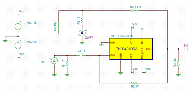
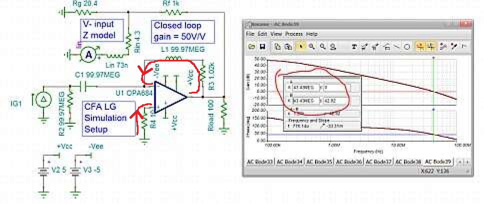
hey Owen, I was starting to look at this, having some trouble with the product folder models, The RGT does not want to operate correctly and DDA looks better, but needed some tricks to get rid of numerical chatter - Anyway, the 1st thing you need to do to run a loop gain sim is to extract the open loop inverting impedance. This set up does that, where the feedback Inductor opens up on the 1st AC step and the large C shorts out. What is there at DC closes the loop and finds a good DC operating point. So this is showing 23.6dBohms at DC (15ohms)with an inductive zero at 500MHz. That implies a series L of 4.8nH.
Then what you need to do is add this impedance at the summing junction in a LG sim with the sense current meter on the other side of that. Here that simulation is showing about 134MHz LG=0dB crossover with 78deg phase margin - you have scaled the R's up which will overcompensate the design.
Here is a V9 file of this, but again I had trouble getting this to run and used some V11 features you may not have,
I'm so sorry that I can't understand the path of input bias currents. Could you please draw the path for me with the different methods. Thanks for your help!
Yes you are right. In your article, the CFA with a closed loop buffer has bigger parasitic inductance. And I wonder, if I want to simulate CFA, do I need to extract the open loop inverting impedance even it's a open loop buffer?
parasitic capacitances of layout will play an enormous role on bandwidth. The same is true for the unavoidable self capacitance of SMD resistors. Because of this the simluation with ideal layout and ideal resistors might not give the higest bandwidth
What circuit do you want to simulate? The inverting or non-inverting amplifier?
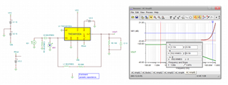
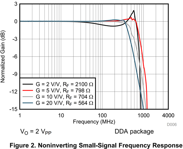
This was measured using the eval board and a network analyzer - with that data then taken into Excel to normalize the plotted data. The peaking gain of 2 plot seems to be hitting a slew limit with that discontinuity
The CFA with internal closed loop buffer has a bigger parasitic inductance which could lead to the gain peaking. But THS3491 with open loop buffer, the gain peaking is caused by hitting a slew limit. Am I right? And as for the black thread, the feedback transimpedance(FT)=2*15+2100=2130Ω, which is biggest and should have the smallest BW, means that the point of F-3dB should be on the left of others, why it's not?
I'm so sorry that I can't understand the path of input bias currents. Could you please draw the path for me with the different methods.
The input bias currents are flowing this way:
Keep in mind that the component in the feedback loop must be an inductance. So your R2 in your very first picture should actually be an inductance and not a resistor