This thread has been locked.

If you have a related question, please click the "Ask a related question" button in the top right corner. The newly created question will be automatically linked to this question.

AFE030: How to initialize the AFE030

Part Number: AFE030
Other Parts Discussed in Thread: AFE031

Hello,

We want to configure the AFE030 to use the Two-wire interface to work in PWM mode. But

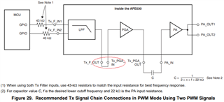
1. Connect one serial port output TX of MCU to E-TXIN, and connect 100KHz PWM waveform generated by MCU  to E_Tx_CLK, but no E_Tx_OUT And gate output  in TX function block of Two-wire.

2. Connected the above PWM square wave to Tx_PGA_IN, there is no output of Tx_PGA_IN, and it indicates that  DAC has not been disabled.

3.Connected the above PWM square wave to Tx_F_IN1,it could see the PWM square wave with reduced amplitude in Tx_F_OUT, but PA_OUT  has no output.

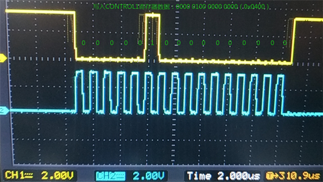
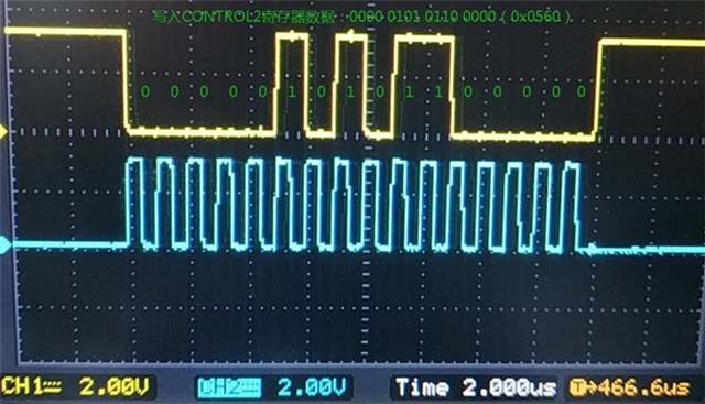
The printed log is as below:

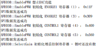
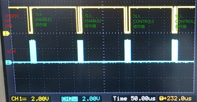
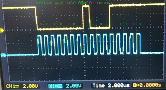
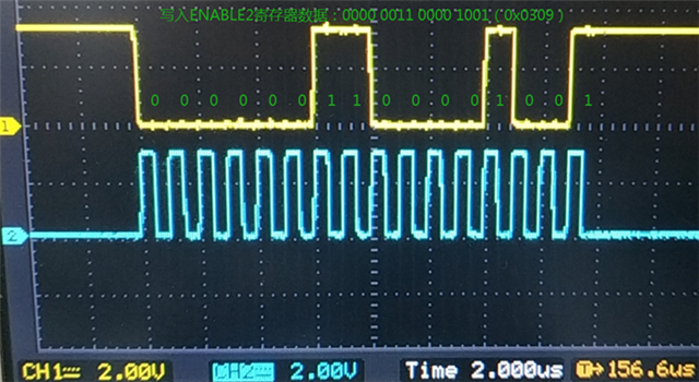
In the brackets are the register addresses, followed by hexadecimal data is the MCU  sent to SPI_DO bus data, after the MCU sent successful interrupt  program will print "SPI data sent successful message".

The MCU provides two types built-in SPI software and hardware interfaces and also provides the SPI underlying drivers: SPI_Master and SPI_Slave.We select SPI_master. Assuming AFE030 is a Slave SPI.

Before initializing AFE030, the program sets the SD and DAC to zero and stays the same throughout the whole  initialization .

Considering  the endian of the data sent, we even tested the 16bit configuration data by reversing the order of the bytes sent, and found the same results whether the MSB were first or last.

So the questions are as following:

1.If the SPI of AFE030 is designed as a slave as we assuming.

2.If the SCLK should be connected together (provided by MCU)?

3.We could see that there is data on SPI_DOUT of AFE030,  which is the same as the configuration data.So it seems that AFE030 responds to the received data ,but it didn't describe this in AFE030 datasheet, and this indicated that AFE030 could receive the configured data correctly.

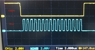
Below are the tested waveforms:

AFE030PWM功能方框图 (2).xlsx

  • Hi Kailyn,

    Please see the attached links that may be helpful for your application. 

    https://www.ti.com/lit/an/sprac94c/sprac94c.pdf?ts=1624320114721&ref_url=https%253A%252F%252Fwww.google.com%252F

    https://www.ti.com/lit/ug/sbou133/sbou133.pdf?ts=1624320381747&ref_url=https%253A%252F%252Fwww.google.com%252F

    1.If the SPI of AFE030 is designed as a slave as we assuming.

    I think that you assumption is correct. If you want to assume that MCU is operating as Master and AFE030 is operating as slave, that will be ok. In PLC application, each PLC board has MCU, and SPI is only communicated between MCU and AFE03x. All other communication signals are coupled onto PLC powerline. So the Master/Slave distinguish is not very important in this case. 

    2. Connected the above PWM square wave to Tx_PGA_IN, there is no output of Tx_PGA_IN, and it indicates that  DAC has not been disabled.

    DAC is disabled via AFE030's Register  -->  Please also see the attached Word file.

    3.We could see that there is data on SPI_DOUT of AFE030,  which is the same as the configuration data. So it seems that AFE030 responds to the received data ,but it didn't describe this in AFE030 datasheet, and this indicated that AFE030 could receive the configured data correctly.

     Please also see the Word file. Please select one of two SPI mode for SPI communication. The SPI mode operation is all configured via software. As long as the rising and falling edge and timing requirements are met the definition, either in SPI mode 0, 0 or SPI mode 1,1, it should work. 

    When Rx data is received, it goes through the passive BP filter first, then go through Rx receivers' gain stages and internal LPF, and then directly sampled by ADC of MCU for signal demodulation (to seperate "1" and "0" via FSK modulation). It does not return to SPI's interface --> to the MCU. So SPI interface is only used to manage the control registers in this case. PWM data is sent directly from MCU to AFE031's PWM input ports directly as well for your two-wire PWM input application --> go through multiple LPF filter to smooth out edges (harmonics) of PWM signals. The output signals are represented by "1" or "0"  by unique transmitter frequency in sine wave via AFE03x's power amplifier. 

    Please take a look at the link below. AFE030 and AFE031 are pin to pin compatible parts. 

    https://www.ti.com/product/AFE031#design-development##software-development

    https://www.ti.com/lit/ug/sbou223/sbou223.pdf?ts=1624321814043&ref_url=https%253A%252F%252Fwww.google.com%252F

    AFE030 Register settings 06212021.docx

    By the way, what MCU are you selecting. If you select C2000 processor, the support is done via C2000 team. Currently, we have many other MCU available to support FSK PLC application, such as TMS320F280025C. And you may download the sample code directly via the application site. 

    https://www.ti.com/lit/ds/symlink/tms320f280025c.pdf?ts=1624322078790&ref_url=https%253A%252F%252Fwww.ti.com%252Fproduct%252FTMS320F280025C

    Please let me know if you need additional help. You may also contact me directly via the internal email.

    Best,

    Raymond


  • Hi Raymond,

    Thank you so much for your comments which includes rich information.

    By reading some materials you mentioned in the reply (AFE030 Register settings 06212021.docx and sprac94c.pdf), We didn't find where we have done wrong for the initialization except for SPI mode selection (SPI Mode 0,0 and SPI Mode 1,1 and Standalone Mode)  on which the AFE03x datasheet does not provide any selection information, so we didn't do anything about the SPI Mode selection. Probably this is the reason of our initializatioin failure.

    So should you please give more infomation on the two SPI Modes and .the Standalone Mode: The definitions, the way of selection and in which situation one should use which mode.

    Many thanks

  • Hi Kailyn,

    Please make sure that the SPI interface is meeting the timing requirements, see below. The SPRAC94 app note is the best resource we have. The MCU interfacing with the AFE03x just needs to meet SPI mode 0,0 or 1,1. There’s no pin or register to config on the AFE03x device.

    Normally, you call the subroutine in the list below and there should not have much issues, if you are using the C2000 based processor. If you are using 3rd party MCU, you just need to make sure that the logic timing requirements are met. 

    In the link below, you can download the sample code -- dacmode sample code should have SPI configuration in one of C2000 processor. 

    https://www.ti.com/lit/an/sprac94c/sprac94c.pdf?ts=1624486299331&ref_url=https%253A%252F%252Fwww.google.com%252F

    https://www.ti.com/tool/TIDA-060001

    If you have additional questions, I can ask C2000 team to assist you. 

    Best,

    Raymond