Other Parts Discussed in Thread: AFE031
Hello,
We want to configure the AFE030 to use the Two-wire interface to work in PWM mode. But
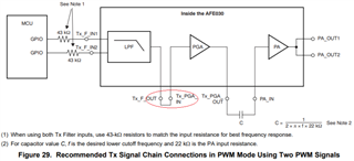
1. Connect one serial port output TX of MCU to E-TXIN, and connect 100KHz PWM waveform generated by MCU to E_Tx_CLK, but no E_Tx_OUT And gate output in TX function block of Two-wire.
2. Connected the above PWM square wave to Tx_PGA_IN, there is no output of Tx_PGA_IN, and it indicates that DAC has not been disabled.
3.Connected the above PWM square wave to Tx_F_IN1,it could see the PWM square wave with reduced amplitude in Tx_F_OUT, but PA_OUT has no output.
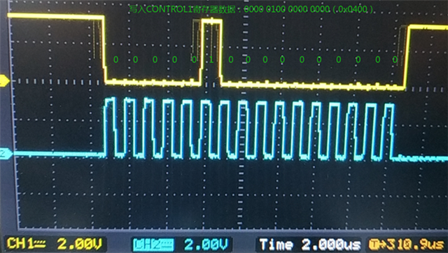
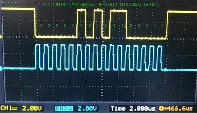
The printed log is as below:
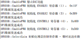
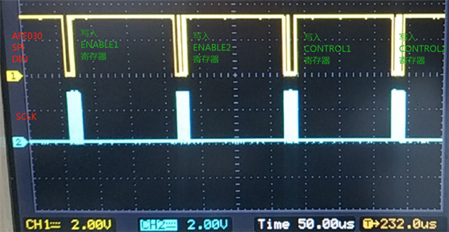
In the brackets are the register addresses, followed by hexadecimal data is the MCU sent to SPI_DO bus data, after the MCU sent successful interrupt program will print "SPI data sent successful message".
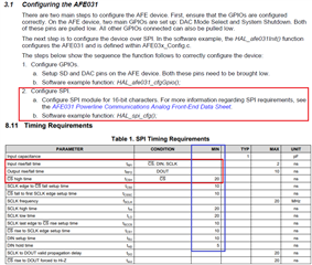
The MCU provides two types built-in SPI software and hardware interfaces and also provides the SPI underlying drivers: SPI_Master and SPI_Slave.We select SPI_master. Assuming AFE030 is a Slave SPI.
Before initializing AFE030, the program sets the SD and DAC to zero and stays the same throughout the whole initialization .
Considering the endian of the data sent, we even tested the 16bit configuration data by reversing the order of the bytes sent, and found the same results whether the MSB were first or last.
So the questions are as following:
1.If the SPI of AFE030 is designed as a slave as we assuming.
2.If the SCLK should be connected together (provided by MCU)?
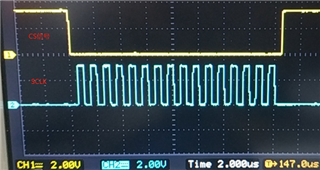
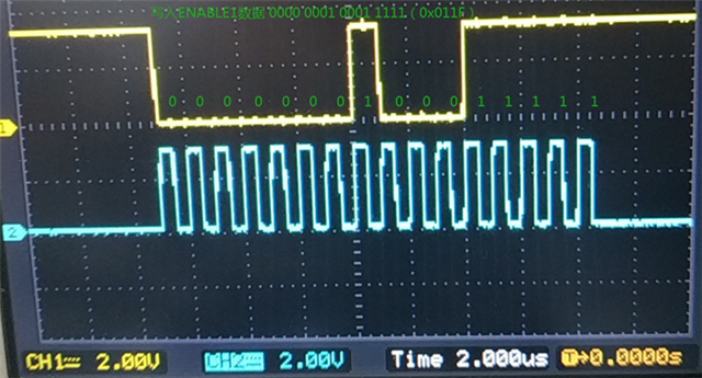
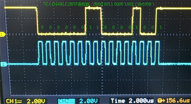
3.We could see that there is data on SPI_DOUT of AFE030, which is the same as the configuration data.So it seems that AFE030 responds to the received data ,but it didn't describe this in AFE030 datasheet, and this indicated that AFE030 could receive the configured data correctly.
Below are the tested waveforms:
