This thread has been locked.
If you have a related question, please click the "Ask a related question" button in the top right corner. The newly created question will be automatically linked to this question.
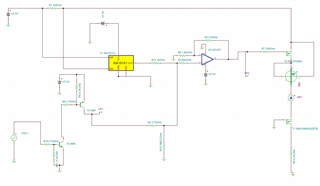
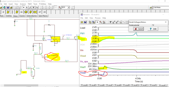
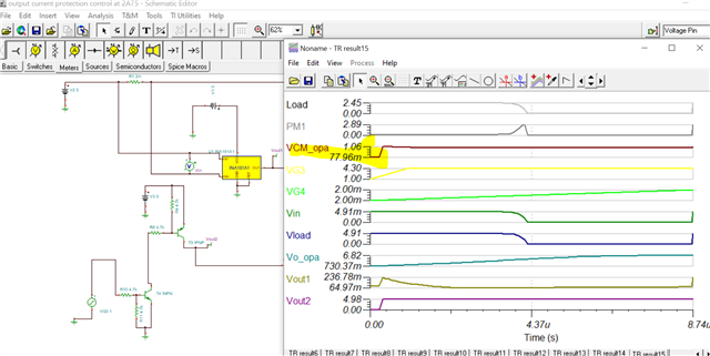
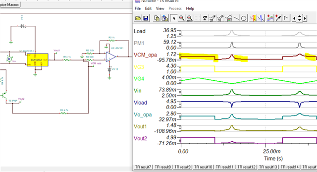
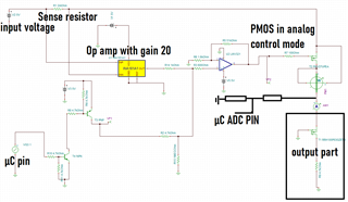
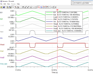
2068.output current protection control at 2A75.TSC
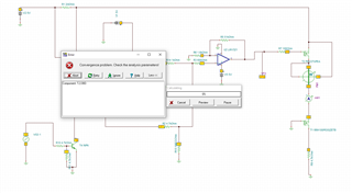
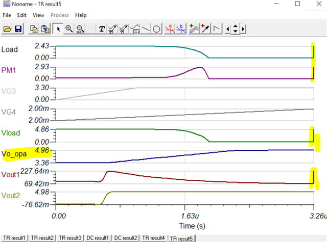
I developed some circuitrary but I am getting error of convergence problem. I checked all circuit parameter but still the error present. Can you please tell me what exactly this error message means ? and how to resolve such issues?
Hey Saurabh,
Looks like the convergence error is with U1.
I have changed the assignment of the ticket to the current sensing team.
All the best,
Carolina
Hello Saurabh,
Welcome to our Forum. Thank you very much for the simulations.
I can get stable DC voltage simulations, but the transient seems to involve PWM feedback loop with. I added a few meters to give sim context. But it seems like VCR is controlling load very quickly and the output of the op amp (LMV321) is slamming into is 5V power supply and thus is saturated, which will cause output delay and thus overall loop delay to control waveform.
Note that there is a way you can still see the simulated waveforms up until they did not converge. It seem like convergence breaks down when the controlling PWM signal tries to shift the load from 0A to 2.43A See below.
In below failed convergence sim waveform plots, the input VCM to op amp (LMV321) is being held at 1.06V and so op amp attempt to gain it to 51V based upon schematics op amp gain. The reason is that VG3 is turning on a pnp that is pulling op amp VCM to ~5V.
I actually got the transient simulation to work with two different ways. Change the DC bias of VG3 to 3.3V or Change LMV321 feedback resistor to 1kOhm. I believe the first solution works because VG3 is not saturating the output of LMV321 by pulling its input pin up to 5V essentially. The second fix which I believe to be more desirable just reduces the op amps closed loop gain to approximately 1.
Best regards,
Peter
Hi Peter,
Thank you so much for your reply.
I wanted turn off the PMOS completely from the VG3 when required (will be coming from µC pin which has 3.3V as logic high) and for the current control I need to have opamp with high gain. As you wrote it works perfectly fine in steady state as well as in open loop gain but unfortunately It shows error in close loop.
Can you please guide me in this.
Regards,
Saurabh
Hey Sarah,
I am confused when you mention things like steady state and open loop gain because these are not the issues causing your circuit to fail. It is difficult to design a control circuit when I am not sure what requirements are.
If you want to be able to turn off the PMOS using VG3, then the circuit you have to in fact do this; however it does it at the expense of saturating your op amp output, which will cause saturation delays in the op amp and this delay gets worse as the closed-loop gain of op amp increases. The delays will cause problems when you are periodically switching VG3. It is necessary to do this?
If you could find a way to turn off and on the PMOS with VG3 quickly without saturating the OPA, then you may want to start there so you can keep these two things independent of each other.
I would recommend compartmentalizing your circuit. Maybe add another op amp that takes the signal from VG3 to turn off the PMOS so this switching circuit is independent to your current-control loop.
If you need more help, please send a description of circuit's purpose and operation and control loop timing requirements, as well as the basic current sensing requirements needed by the INA181. I need to know what you are actually trying to simulate so we can make sure the transient simulation is relevant. If you wish to send this information to me privately, you can do that over a private message here or at my email: p-iliya@ti.com.
Best,
Peter
Hi Peter,
Thank you so much for your reply. I am planning to design output current control circuit. In case of fault (over current) which should be cut down using microcontroller pin. Which has logic high of 3.3 V. There will be one voltage divider which will be use to give voltage to adc of µC. PMOS is in After the PMOS there is a output part (Output part will be on another PCB) . At the otuput part it is necessery to have more than 4.8V as on output pcb another µC is present.
please find the photo attached for better understanding if you have any questions please let me know. If you know any other technique which will work please let me know.
Regards,
Saurabh
Hey Sarah,
So if you just need to detect an overcurrent condition, then all you may really need is either MCU for a digital solution or a comparator for an analog solution. Refer to these documents and article on using comparator to set the overcurrent signal, which would shut off the PMOSFET.
https://www.ti.com/lit/an/snoaa21/snoaa21.pdf
https://www.ti.com/lit/an/sboa349/sboa349.pdf
You could use a device with an integrated comparator as well such as the INA300, INA301, INA302/INA303, or INA381.
Here is a link explaining why using the LMV321 as a comparator might not be a good idea:
You will have to consider other system requirements on how fast system should come out of or correct overcurrent condition. I am not sure if this is a requirement, but given you have a lot going on in your simulation I will suggest it.
My recommendation is to simplify you simulation. Maybe just one sim to run a DC sweep of the output part's load current to see where the FET will turn off and if this is the correct overcurrent condition. Once this is established, then try running transient simulations.
Sincerely,
Peter
Hi Peter,
Thank you for the reply. We have secondary requirement of circuit is that we want to use same circuit for inrush current protection due to this. we will have to use PMOS in analog region.
I think your suggested techniques will not able to provide inrush current protection function.
If you have any different technique or simulation problem solution in mind please let me know.
Regards,
Saurabh
Hey Saurabh,
Ok well there are techniques to do this. First, I don't think VG3 is needed for testing in-rush, all I believe you would need is a load generator in TINA to simulate a load with a high peak current. Like I said before, VG3 is causing the input VCM of LMV321 to rail and this is saturating the op amp so you don't need to test this in TINA.
Once you have this, then you could perform stability analysis with the LMV321 it's feedback through the PMOS. So here is the simplified circuit with the load set to a triangular wave from 0A to 6.6A. According to simulation, the op amp will turn off PMOS at around 5A.
Once you have this circuit reacting like you want, then you will need to break open the op amp's loop and refer to the following videos to determine stability performance.
I would recommend starting a new thread focusing on checking circuit stability so we can get you the right folks to help.
Sincerely,
Peter