Because of the holidays, TI E2E™ design support forum responses will be delayed from Dec. 25 through Jan. 2. Thank you for your patience.

This thread has been locked.

If you have a related question, please click the "Ask a related question" button in the top right corner. The newly created question will be automatically linked to this question.

OPA858: A switched transimpedance circuit (simulation Pspice for TI)

Part Number: OPA858
Other Parts Discussed in Thread: TMUX1122, TINA-TI

Hello,

I am working at the software Pspice for TI, and I am designing a transimpedance circuit for photodiode sensing. My design demands many times of measure repeatedly (with a period at about 2us).
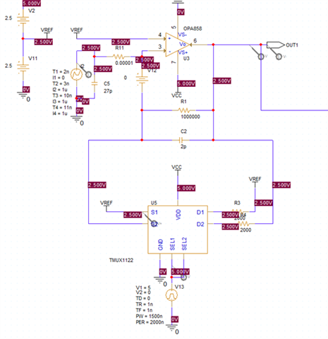
In the circuit, there is a T-gate switch which will control the gating measure (the TMUX1122, works with negative logic). I2 and C5 is an equivalent model for the photodiode.

In the simulation, V(out1) (the green) shows that the first measure works exactly the same as my expectation how the circuit would work like: 

when the switch is closed, the circuit works as an integrator and the beginning voltage is the Vref (2.5V), and when the switch gets closed, the output reset at 2.5V.

But in the second and third measure, the integration still works but there is a voltage leap when the switch changed and il makes the beginning voltage is no longer 2.5V.

The current source I2 is fixed at 1uA at the simulation.

I suppose that there is some capacitive part keep charged even when the t-gate switch has closed and the voltage between input/output is the same. But I cannot find where it is, I think the C2 would be discharged when Vout = Vin.

Best regards,

Libin

  • Hello Libin,

       I believe your assumption is right. There seems to be a charged capacitor. Would you be able to share the Pspice for TI zipped project folder with us?

    Thank you,

    Sima 

  • Hi Sima:

    Thank you for the reply, here is the zipped file for the Pspice project floder.

    Libin

    opa615.zip

  • Hello Libin,

      Thank you for the Pspice project. It does not look like it has to do with feedback capacitance specifically. Still looking into this and will get back to you by the end of the week.

    Thank you,
    Sima

  • Hello Libin,

       Sorry for the very long delay on this. I have an issue on my end with PSpice for TI that is going through some fixing, so I had to switch over to Tina-TI. The below images/simulations are from Tina-TI, but you can continue using Pspice for TI. 

       It looks like this is an issue with the capacitors that are within the switch. I increased the duration of the pulse (decreased frequency) from 500kHz to 100kHz and the issue went away. This will be a difficult issue to deal with at higher frequencies due to the larger capacitors found in switches. I can move this thread to the switches team at TI to look into this further. But, we should fix the instability issue of the amplifier first.

      A 1ns rise time pulse with a combination of high input capacitance of  27pF and high feedback resistance of 1MOhms is not a feasible solution. If you are unable to lower gain or switch diodes (lower input capacitance), then you would need to use a two stage design. Here is a link to an excel calculator that will give you either the minimum GBW of an amplifier needed to fulfill the system requirements, or will give you the bandwidth of the system which is related to the rise time of the pulse (0.35/risetime). 

      Here is a stable solution using input capacitance of 27pF, feedback resistance of 1MOhms, but a system bandwidth of 5.7MHz.


      Let me know if you need more explanation on TIA design. Here is a good overview video of designing TIAs, and here is a blog series on choosing the right TIA for your application. 

    Thank you,

    Sima