Part Number: OPA322
Other Parts Discussed in Thread: FDC2214EVM, FDC2214, OPA320, LM337, LM317
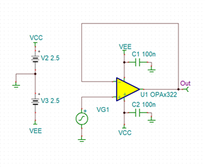
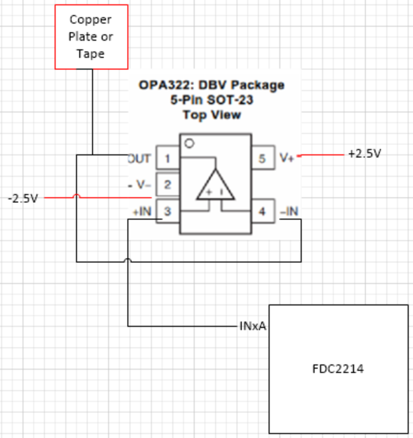
The picture below was proposed by Kristin Jones93 in a thread, whose link is:
In Kristin's opinion, OPA322 was used to work as a buffer so that a shield copper plate can connect with FDC2214EVM.
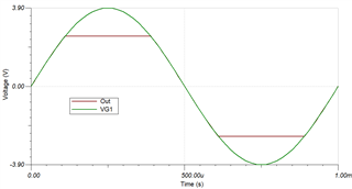
According to this picture, the out of OPA322 should be in phase with its input and its out should be equal to input.
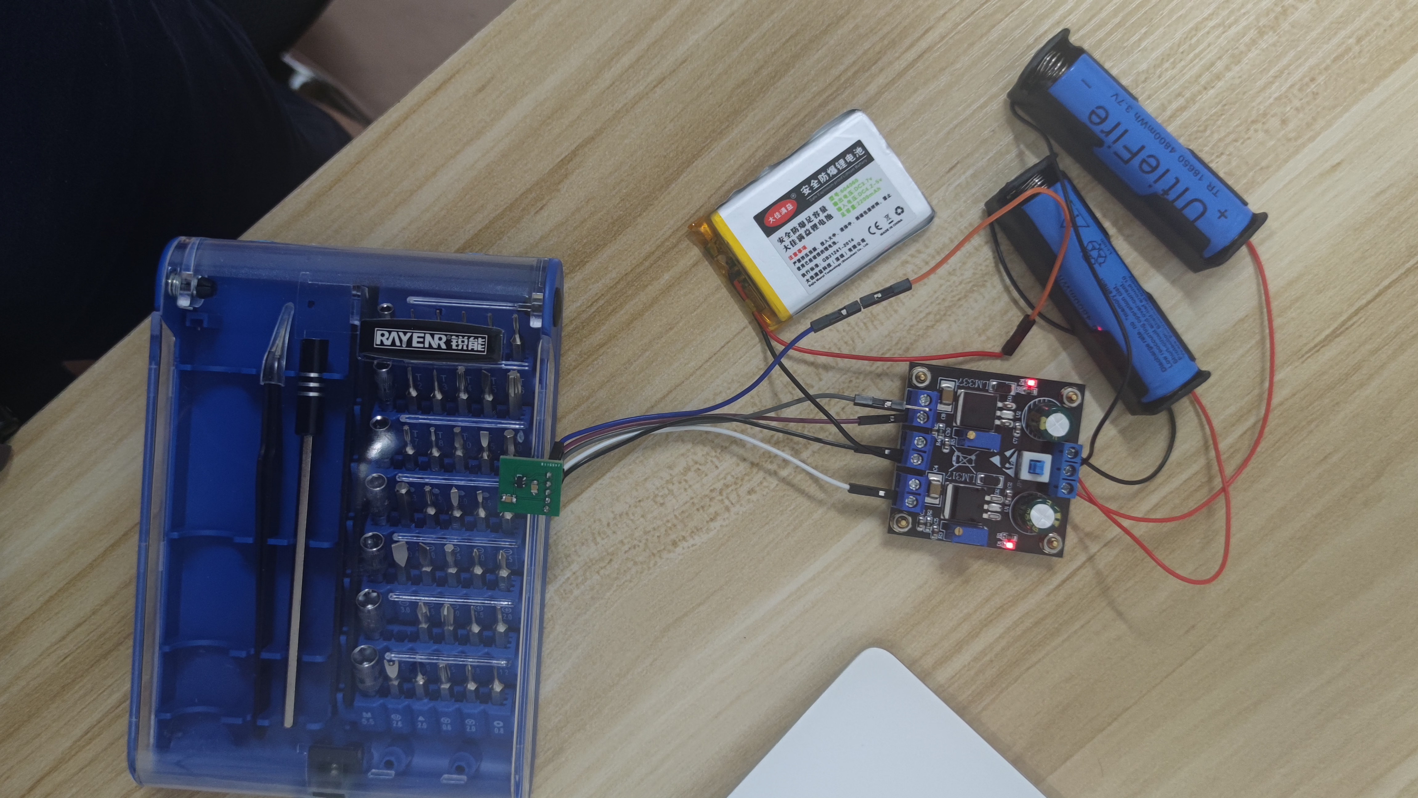
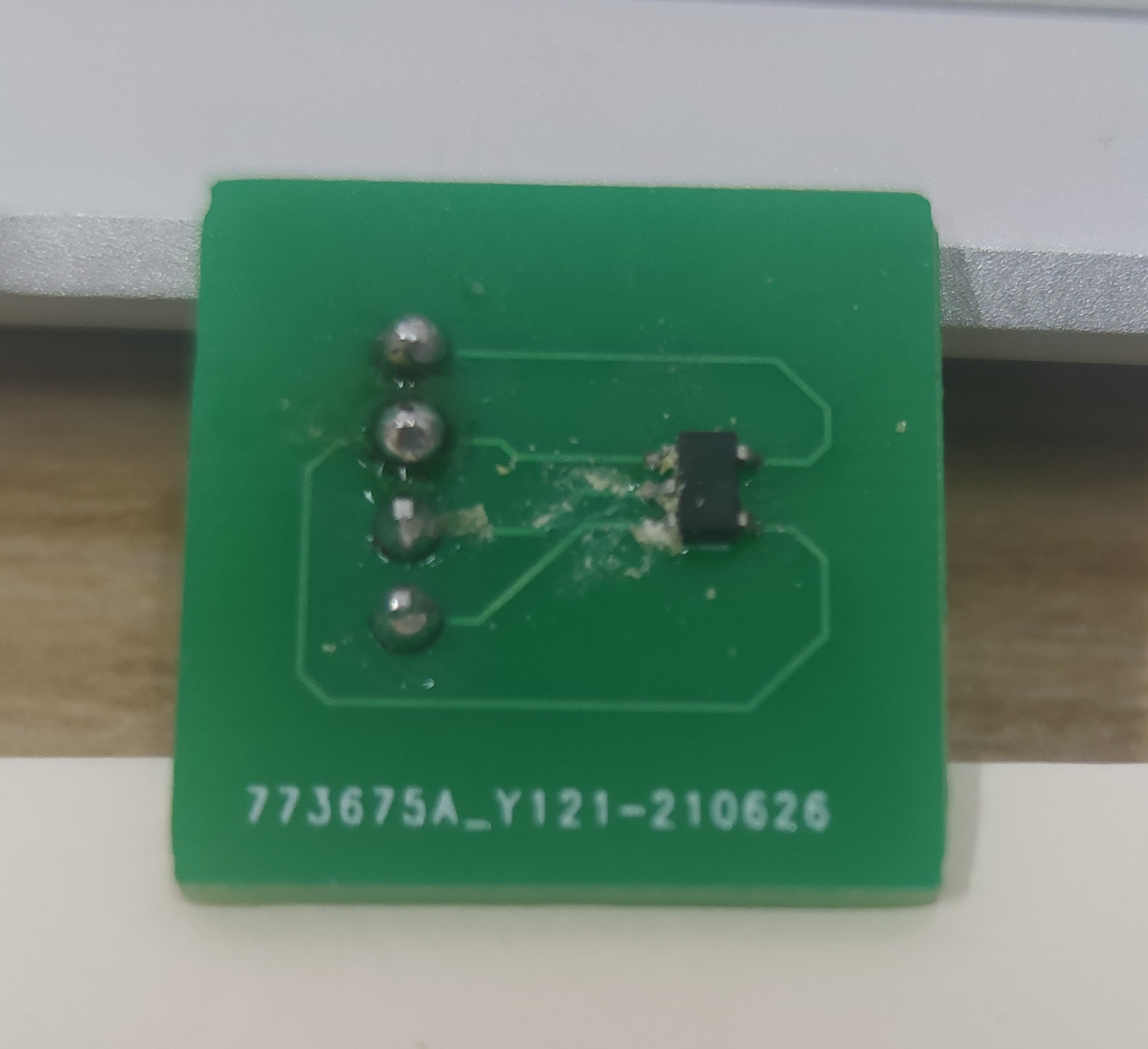
I set up the device and tested it according to the settings on the figure. I purchased OPA322 and weld it on PCB board with welding torch.
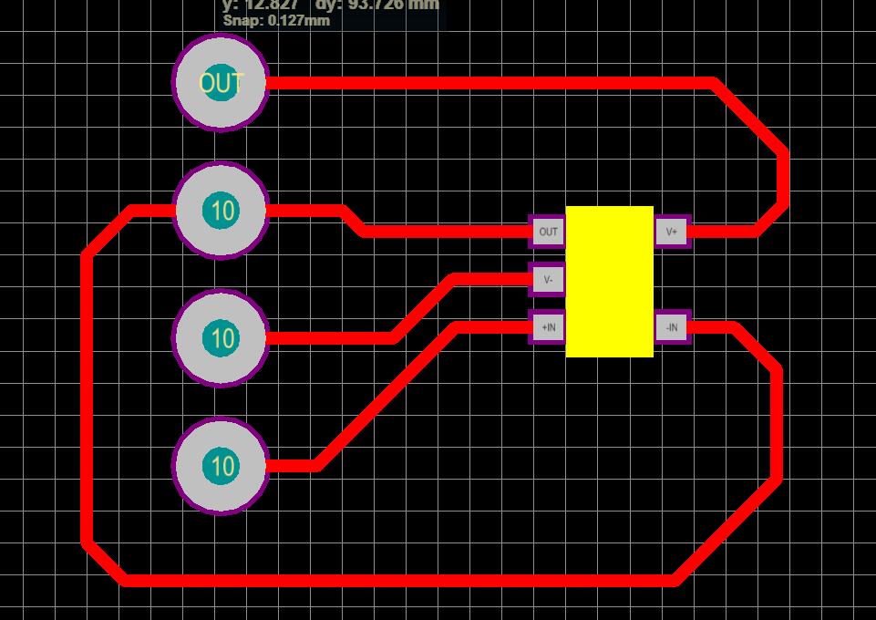
The PCB design drawing is as follows.
The temperature of the torch I use is 300 degrees Celsius.However, I later checked the datasheet of OPA322 and found that the operating temperature of this component is only 150 degrees Celsius at the highest.(I don't know if this is the reason I met?)
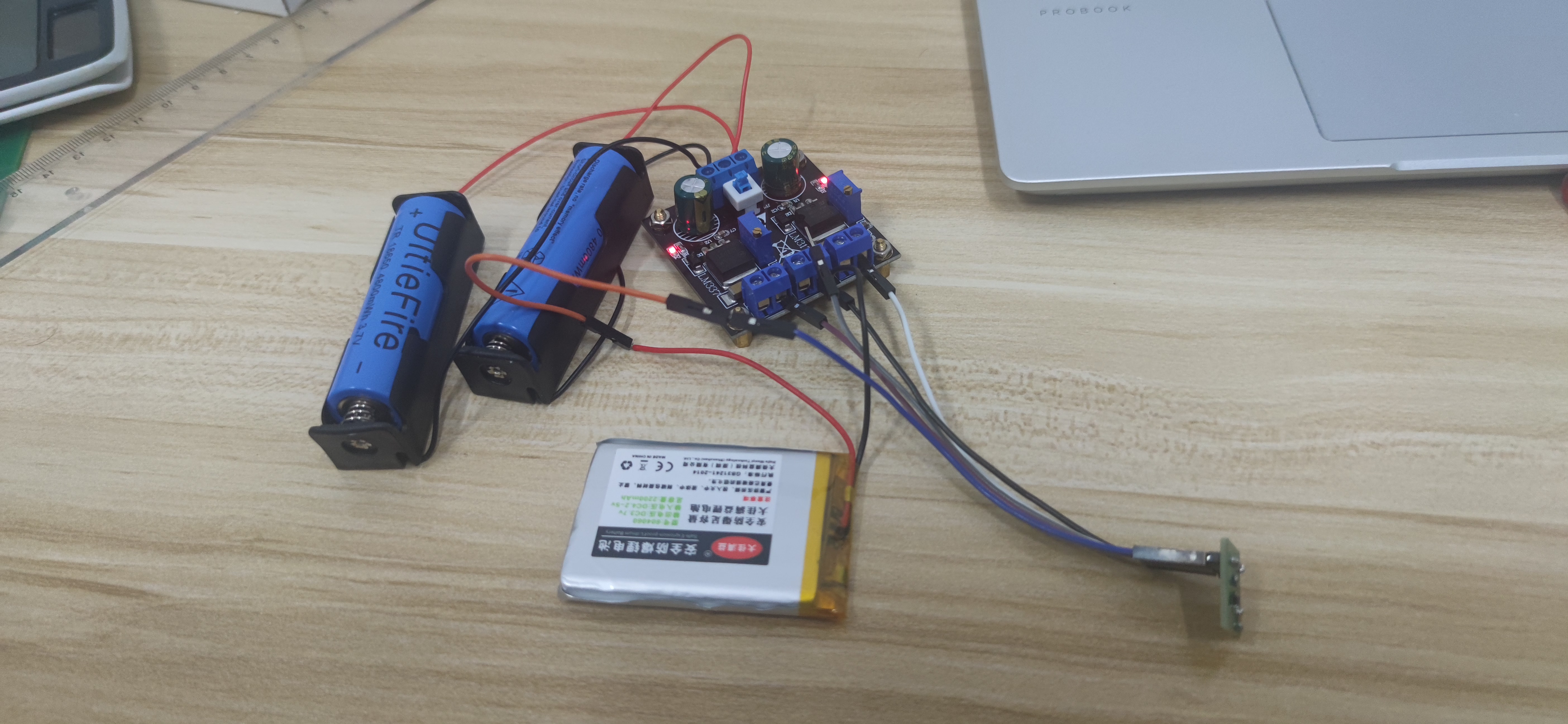
The resulting physical diagram is shown below.
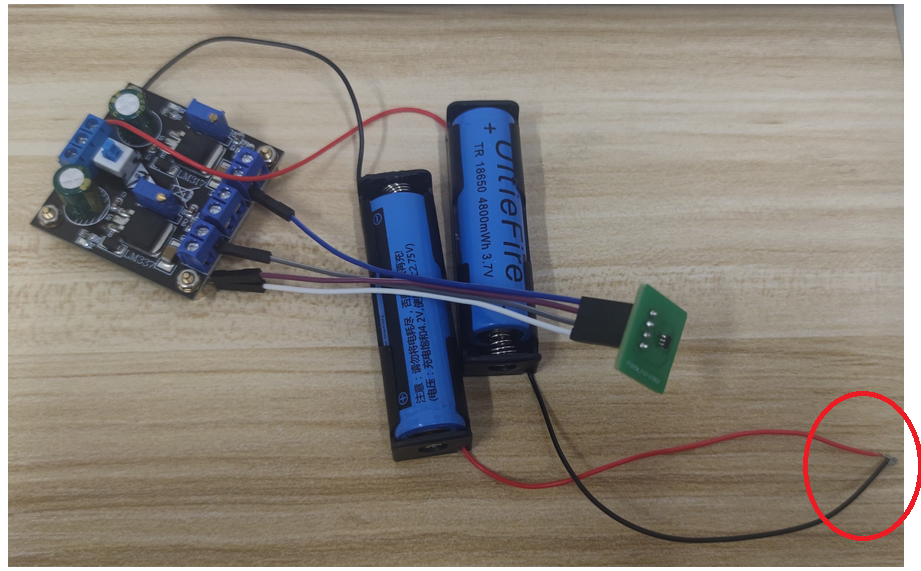
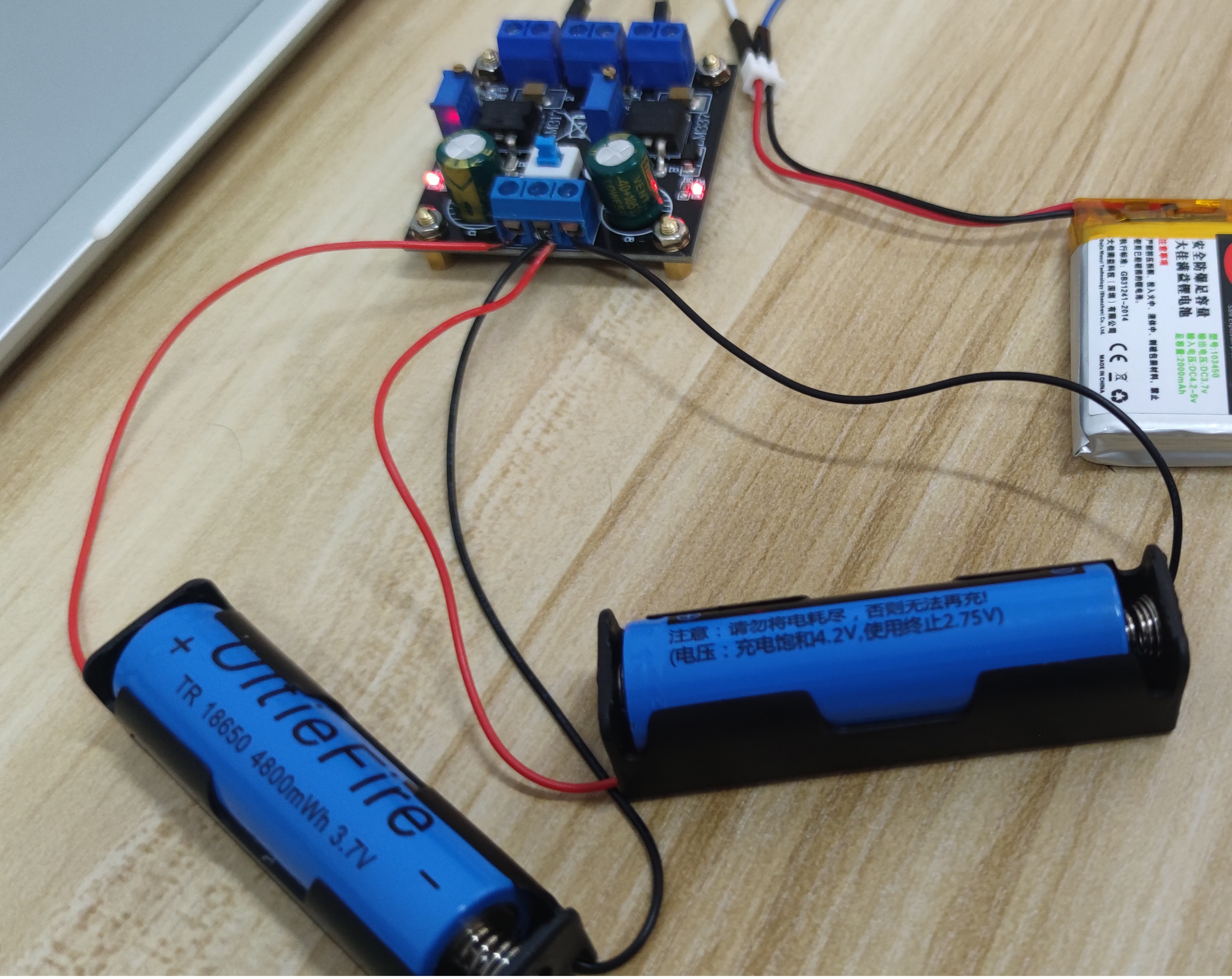
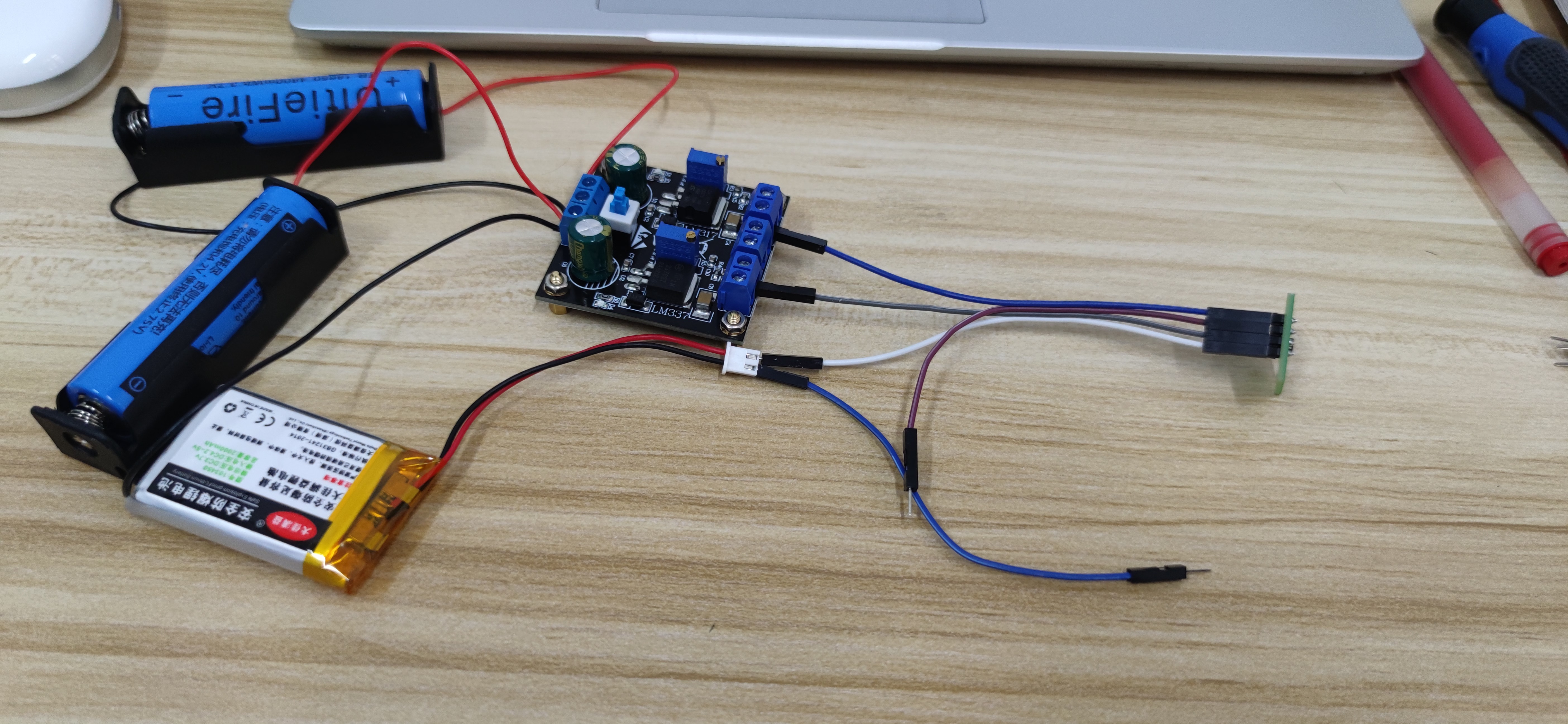
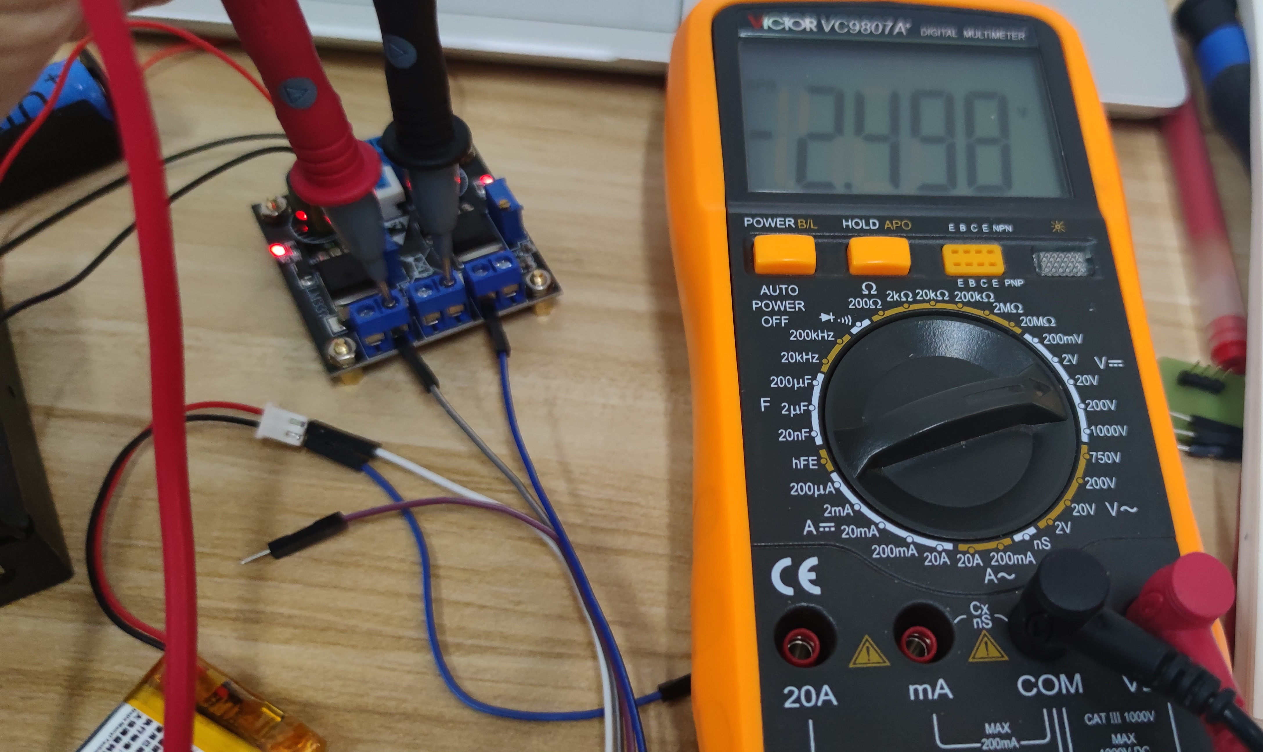
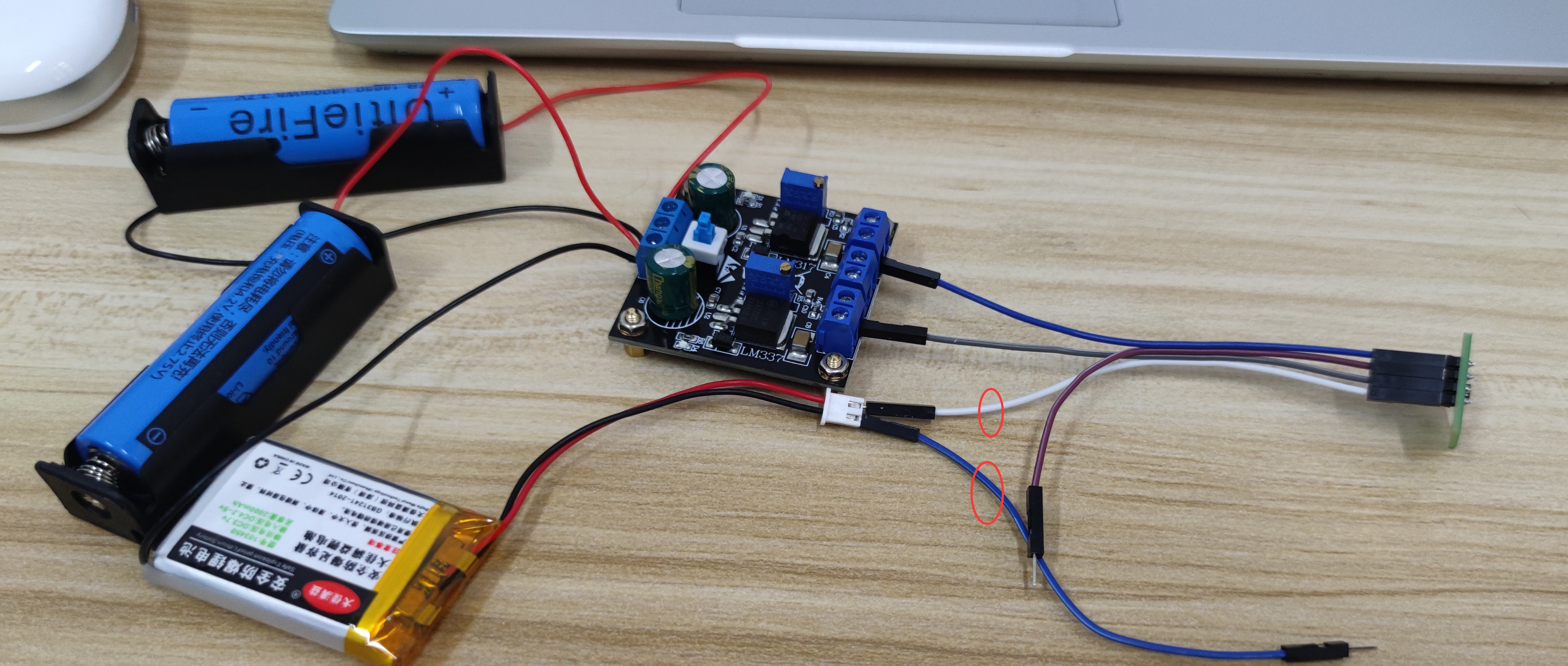
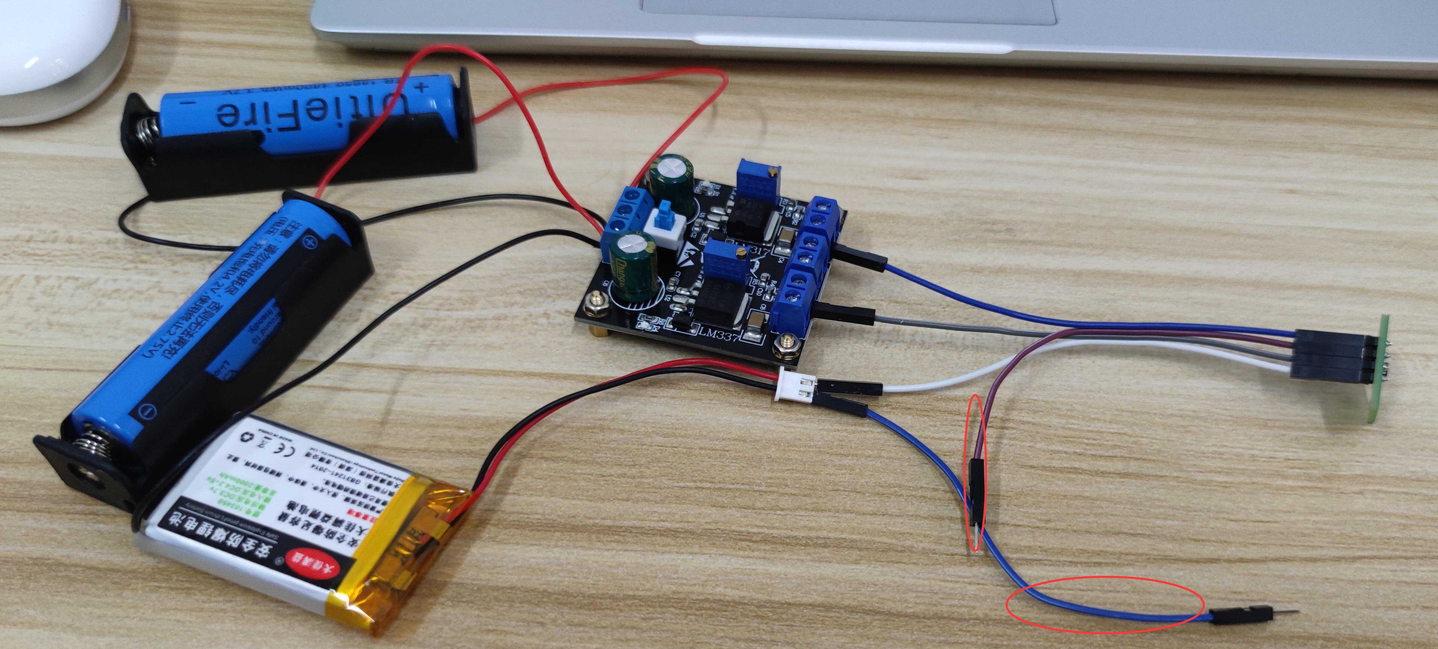
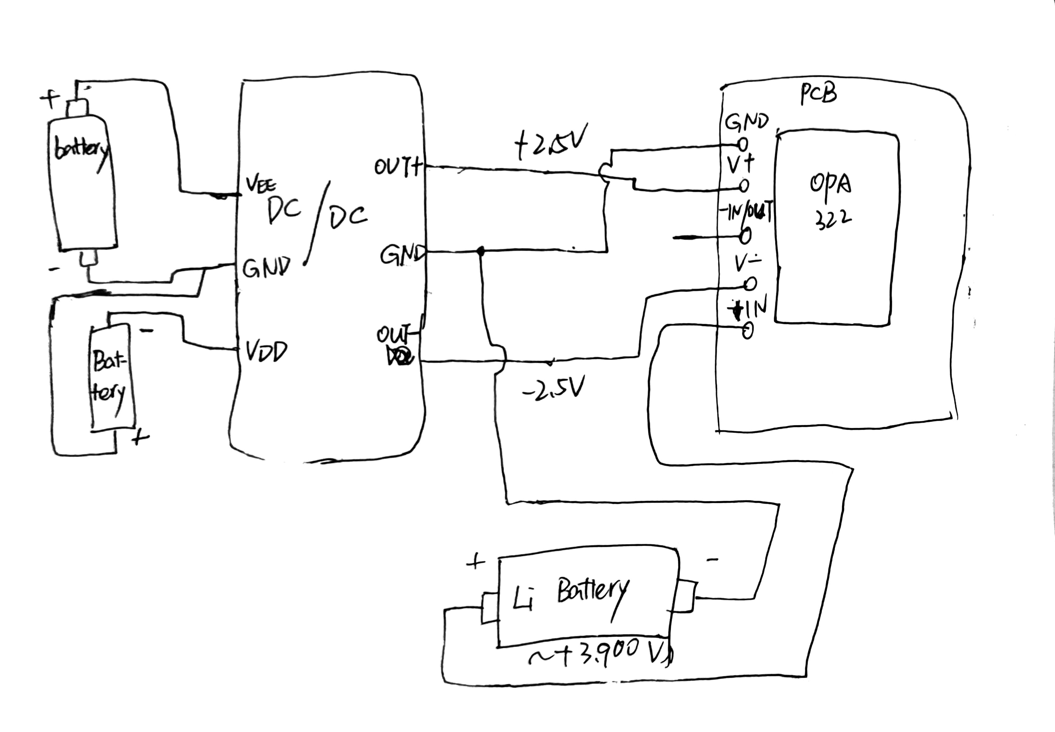
Regarding the +/-2.5V power supply of the components,I used a voltage regulator and 2 lithium batteries to get the required +/-2.5V voltage.
The final connection diagram is shown below.(I have confirmed that the output of the voltage regulator are +2.496V and -2.496V respectively.)
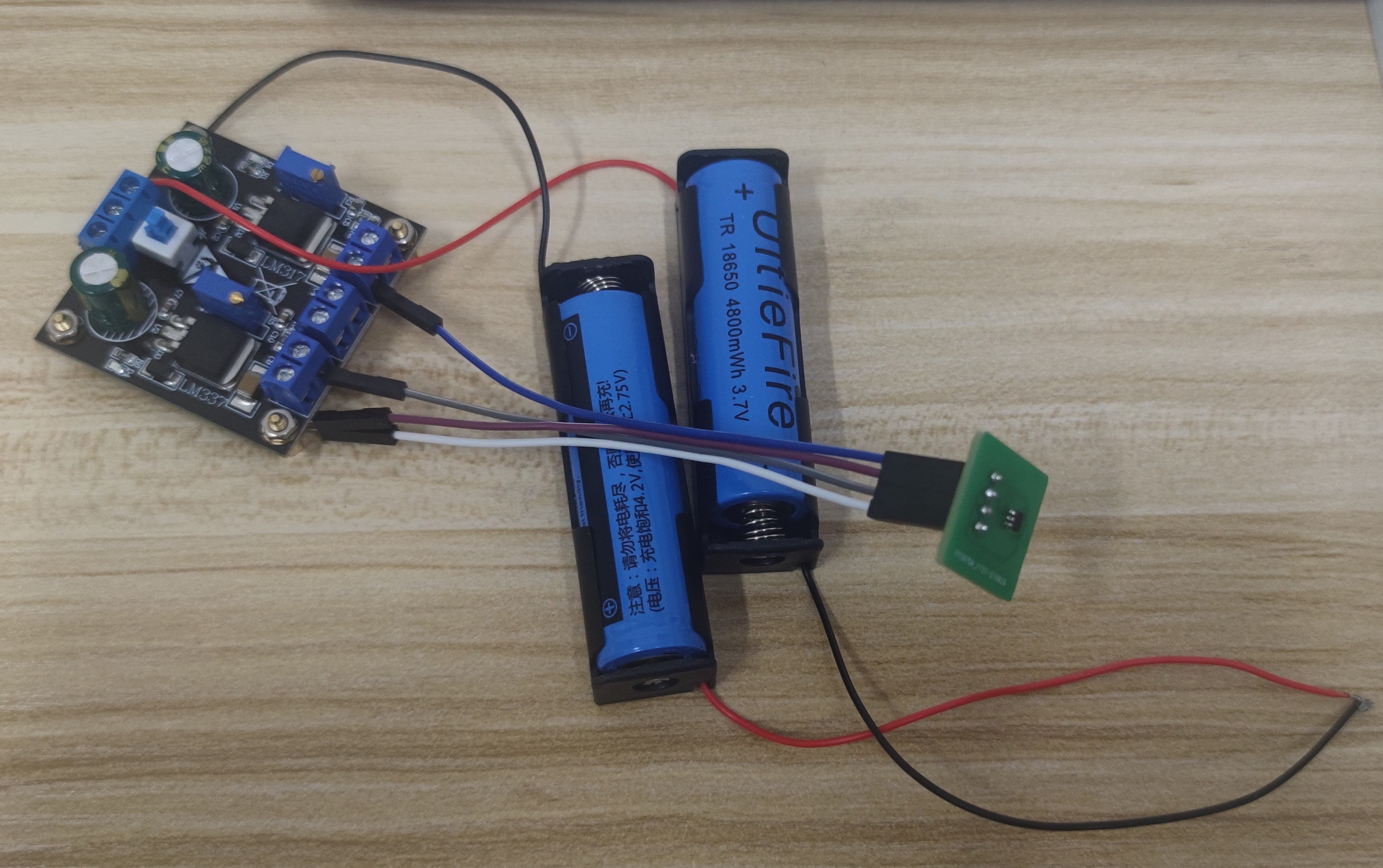
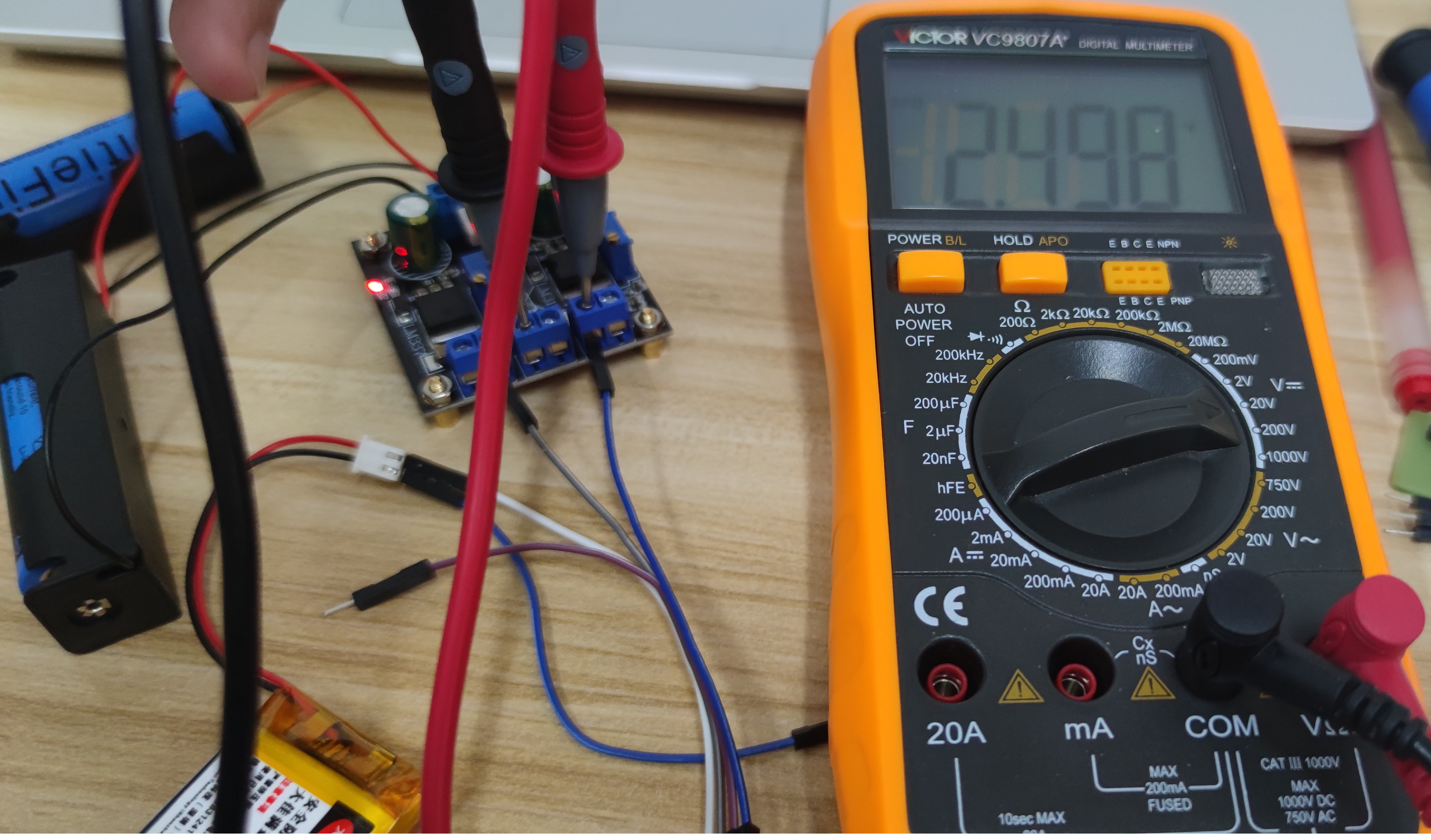
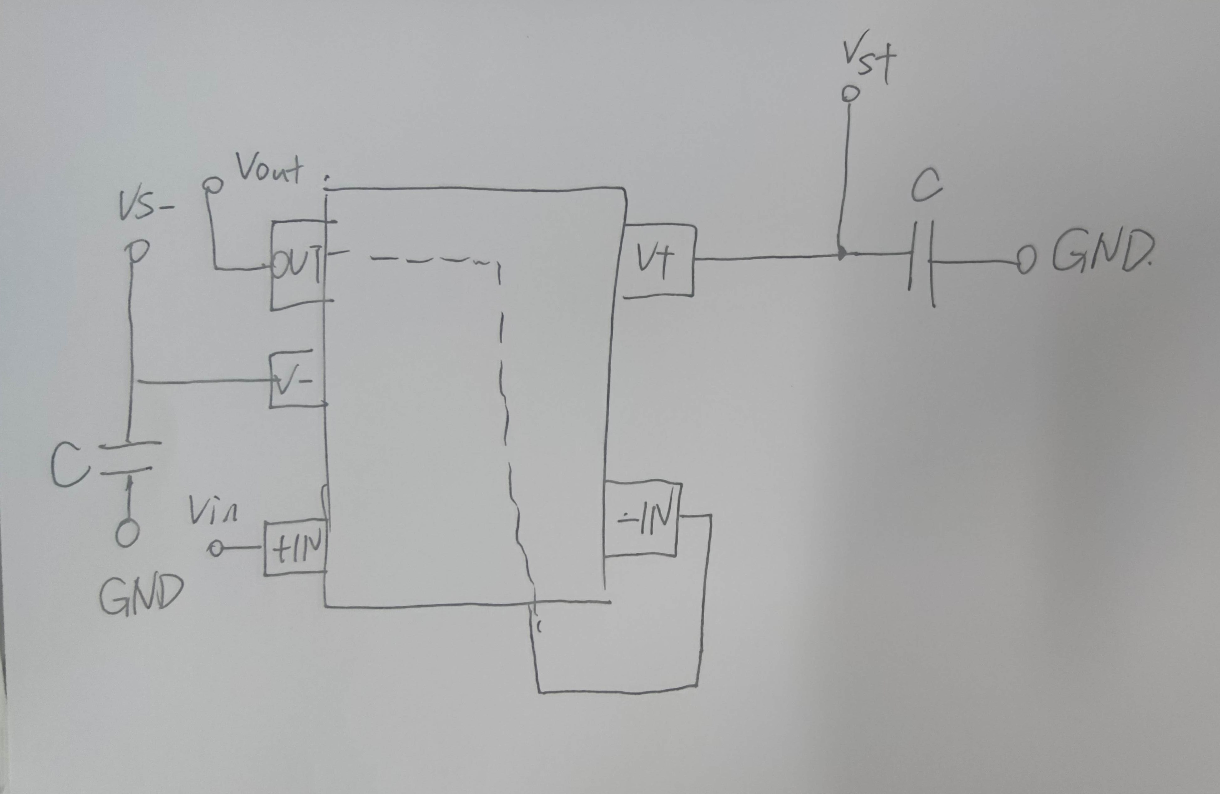
And then I ran a test on another lithium battery. I connected the positive electrode of the battery to the input end of OPA322, while the output end of OPA322 is opening.
The multimeter measurement showed that the voltage between the OPA322 input terminal and the battery negative terminal was 3.742V.
But the voltage between the OPA322 output terminal and the battery negative terminal was 3.228V.
The difference between the two voltages is 0.514V rather than 0V.
My problem:
1.Is the voltage difference normal ?
2.If not, what are the possible reasons for this? And how to solve them?
3."actively driven shield: The shield is a buffered signal of the INxA pin. The signal is buffered by an external
amplifier with a gain of 1." This sentence comes from the datasheet of FDC2214.
For FDC2214EVM, what is the significance of adding such a buffer between the input signal and the shielding electrode?
Since the signals from both the shielding electrode and the sensing electrode are of the same size and phase, why the need for an intermediate buffer? Why not connect them directly?
Regards.