This thread has been locked.

If you have a related question, please click the "Ask a related question" button in the top right corner. The newly created question will be automatically linked to this question.

INA250EVM: INA250

Part Number: INA250EVM
Other Parts Discussed in Thread: INA250

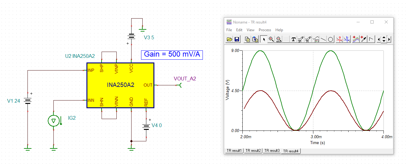
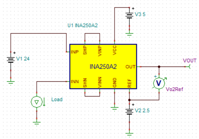
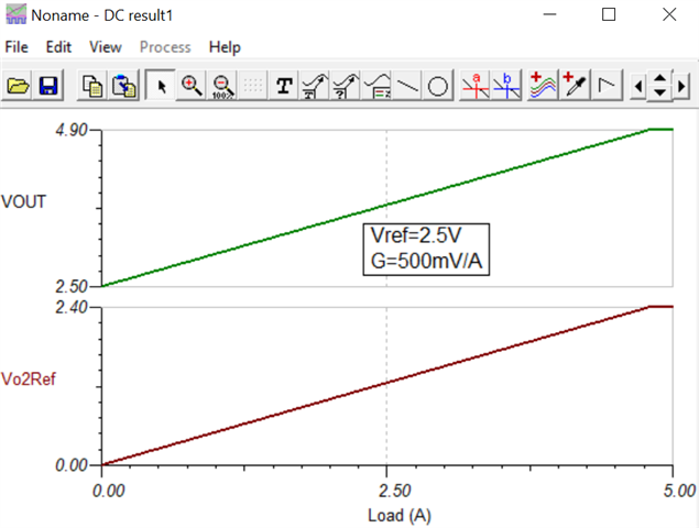
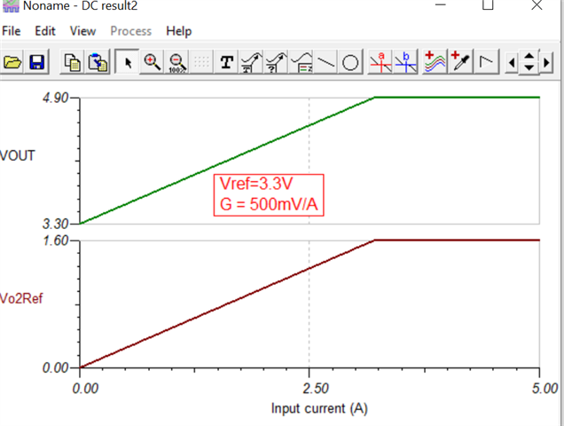
As per the datasheet on page 15 about the amplifier transfer function of INA250 with respect to VREF. https://www.ti.com/lit/ds/symlink/ina250.pdf#page=15.

However, the output is saturated with applied Vref Voltage(2.5V/3.3V). With Vref 0V not seeing any output. 

Case CS0591535 has been Updated - INA250: How does Vref impacts in Output?Ecat distributiontesting.xlsx

  • Latha,

    Is it possible to see your schematic here, and a description of the test you are running here? Also, how are you applying the reference voltage to the REF pin?

  • Vref pin is connected to an external power supply with common ground. Using the below EVM Kit. Just connecting the load and supplying 24V to Vs Pin.

    https://www.ti.com/lit/ug/sbou153a/sbou153a.pdf?ts=1626252991426&ref_url=https%253A%252F%252Fwww.ti.com%252Ftool%252FINA250EVM 

  • Latha,

    In the data you provide above, are you probing the output with respect to the reference? The REF pin takes in a voltage from a low impedance source and translates that voltage as a DC offset to the output pin. If you probe the output with respect to ground, you should see the gained signal from your measurements stacked on top of this provided voltage. If the measurement is taken with respect to the REF pin, only the differential measurement will be shown, i.e. gain*I_load.

  • Output Vs Gnd - Analog output measuring terminals. My question is do we really need Vref if its a Unidirectional (just measure wht is the load is fed across the IN+ & IN-.? Can we eliminate Vref and connect to GND? 

  • When Vref is 0V, for 500mV/A gain not seeing any output as expected. EX: for 5A corresponding output should be 2.5V. Please Suggest on how to proceed. 

  • Latha,

    Got it.

    Kai's sims should be able to help you visualize here. The answer to your question is situational. If you are intending to drive the output to a "true 0V" condition, then typically yes, you will want to provide a reference voltage, even in the unidirectional case, to pedestal the voltage above this condition. If you reference to GND, the output stage will not be capable of truly driving to zero, as you will saturate against the rail of the amplifier before reaching 0V. By providing some small amount of voltage greater than the swing condition, you will allow the solution to drive to the 0V condition and not saturate. There is more information on this topic in this paper

    However, if you do not intend to drive the output below the swing condition, then yes, you may run the device referenced to GND, which is in effect placing the device in a unidirectional condition.

  • Hi , could you please share me the oscilloscope outputs for 1A, 5A  with Vref 2.5V/3.3V? Also, would like to see the switching time and response time for the same.

  • Hey Latha,

    Here are the requested waveforms. I also attached the DC sweeps for load = 0A to 5A for both VREF conditions. As you can see, making your VREF =3.3V will seriously diminish the full-scale range of unidirectional current you can measure. If you want to measure unidirectional current, then you should consider keeping VREF a lower voltage. However, the one key benefit to providing a reference voltage is that you always keep the output in the linear region of operation even when load = 0A. This is important if you are measuring switching currents that can start from and fall to 0A and you need the device to react as quickly as possible to avoid overload recovery delay (which happens with any amplifier when its Vout is saturated into a supply rail and it needs to get out of this saturation). Any VREF >=100mV will work to bias the output into linear region and keep device from saturation at load=0A and thus prevent overload recovery delays.

    Remember the following equation is always true: Vout = Load*Gain +Vref.

    Hope this helps.

    Best,

    Peter

  • Thanks and appreciate the details. With Vref 3.3, observing Vout+3.3V(Vref) with the chip A2 amplifier. Looks something went wrong. 

  • Also, Is there any solution from TI to achieve the  ADC to Isolated SPI ( Target is to connect the INA250 which is non isolated to Isolated SPI - connect 4 to 8 INA250 adc output signals and converter them to SPI signals which is Isolated)

  • Hey Latha,

    Concerning the simulations, nothing went wrong and amplifier model is behaving exactly has it should. They are displaying the point I am making about setting Vref voltage too high. The output voltage of the INA250 (and all other amplifiers) are bounded by their supply voltages. Vout can never exceed supply Vs. When making Vref = 3.3.V, this means the amplifier's Vout can only move from 3.3V to 5V for positive currents, thus output range is diminished. Thus, Vout saturates into Vs rail (minus ~100mV of datasheet swing) at around +3.2A.

    As for the SPI digital isolator, I believe one of our digital isolators can help here. You can view all digital isolators here:

    https://www.ti.com/isolation/digital-isolators/products.html

    You can learn plenty about these products here:

    https://www.ti.com/isolation/digital-isolators/technical-documents.html

    You can also get more information and ask questions to the experts at the following links:

    https://e2e.ti.com/search?q=SPI%20isolation&category=forum&group=355

    https://e2e.ti.com/support/isolation-group/isolation/f/isolation-forum/991655/faq-how-to-connect-spi-mcu-to-multiple-isolated-spi-nodes?tisearch=e2e-sitesearch&keymatch=SPI%20isolation#

    Sincerely,

    Peter

  • I load (A)

    Expected

    Vout (V)

    Actual

    Vout (V)

    0.5

    0.25

    0.253

    1

    0.5

    0.497

    1.5

    0.75

    0.725

    2

    1

    0.982

    2.5

    1.25

    1.247

    3

    1.5

    1.518

    3.5

    1.75

    1.724

    4

    2

    1.971

    4.5

    2.25

    2.232

    5

    2.5

    2.415

    I have Vref =2.5V. and corresponding outputs are tabulated. As per the formula, Vout = (Ioad X Gain)+Vref. My question, Vref =2.5V (considered as base voltage as 0V) which will never reflect in output mean which will never get added to the output. Please confirm. 

  • Hey Latha,

    I am a little confused with the question, but I think I know how to clear that up.

    I assume that your "Actual" measurements are made with respect to the 2.5V reference voltage, correct? A schematic that correlates to the table of data could be helpful.

    Anyway, the data you present makes sense and demonstrates basic functionality, although there is some gain error in your circuit/instruments, possibly from the DC source, ammeter measuring current, or the volt-meter measuring the output.

    With all that being said, to answer your question directly: whenever you drive a reference voltage into the REF pin, the output voltage will become biased up to the DC voltage. So Vout = Gain*Load + Vref (this is with respect to ground). Usually it is helpful to measure the differential output voltage with respect to the REF voltage. The primary advantage in doing this is that the absolute error in the REF voltage is completely negated. So ideally the REF voltage should be 2.5V, but in reality it might be 2.492V. So in order to make sure there is no 8mV offset error to the measurements, the ADC should measure the differential output ( Vout with respect to VREF) so it never sees this 8mV difference.

    Hope this makes sense.

    Best,

    Peter