This thread has been locked.
If you have a related question, please click the "Ask a related question" button in the top right corner. The newly created question will be automatically linked to this question.
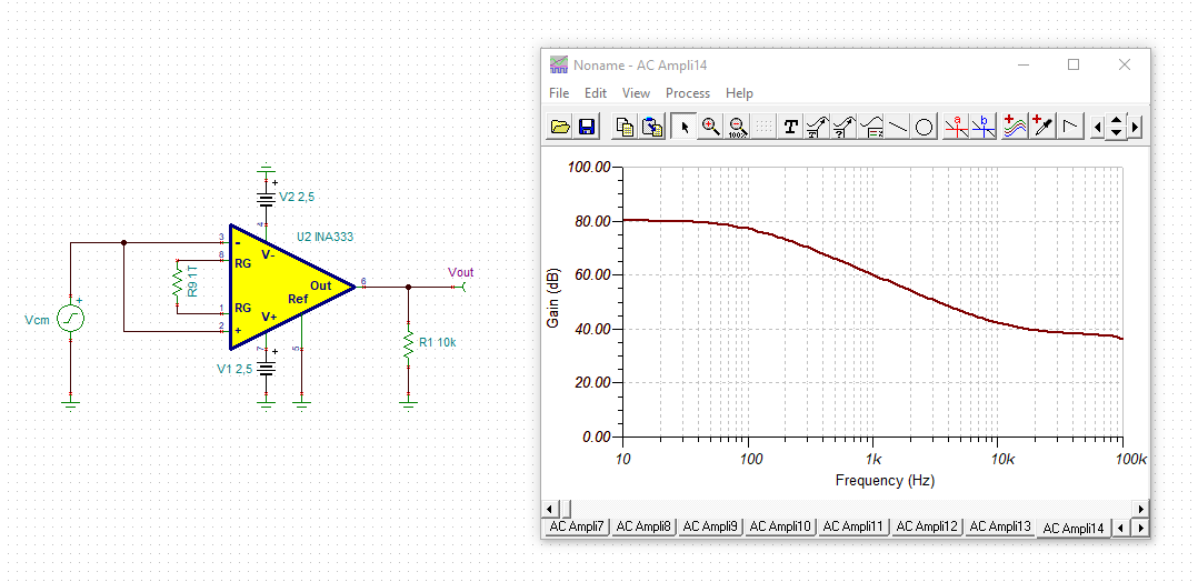
I am trying to simulate the CMRR of my front-end circuit, but noticed that the CMRR plot of the INA333 spice model is different from the one stated in the datasheet. I have attached my circuit and CMRR plot here. I was wondering if you can help me understand why there is a discrepancy between my CMRR plot and the CMRR plot in the datasheet for a Gain of 1? Thank you so much!
CMRR Plot: /resized-image/__size/640x282/__key/communityserver-discussions-components-files/14/INA333G1.PNG
Test Circuit(Gain = 1):
Hi Siddharth,
hhm, with no supply voltage connected and the REF pin floating, you shouldn't be all too surprised that the result looks weird
Also, adding filter elements to the input will change the overall common mode rejection.
With properly connected INA333 the common mode rejection looks very similar to the curve in figure 19 of datasheet: siddharth_ina333.TSC
Please note that I have used the TINA-TI's post-processor to change the sign of common mode rejection plot. Now it looks more like the curve in figure 19
Kai
Hi Siddharth,
Adding to Kai's comments, please see the INA333's CMRR simulation in the thread below.
Best,
Raymond
Hi Kai and Raymond,
Thank you for the initial feedback. Sorry for the miscommunication. I sent the wrong file to you. I have attached the correct file in this message. Unfortunately, I am still running into issues with the simulation of the INA333. I tried plotting the CMRR for a gain of 1, and I am getting a CMRR of around 160 dB in the low frequency range when the datasheet graphs show a gain of 90 db. I have attached the plots from the AC analysis below. Can you help me understand why my simulations yield a higher CMRR than stated in the datasheet? Thank you!
Hi Siddharth,
Can you help me understand why my simulations yield a higher CMRR than stated in the datasheet?
As Kai demonstrated, you need to insert DC biased voltage at the input, since the circuit is adapting a single supply voltage of 5Vdc. This is to place INA333 in the linear operational region.
Best,
Raymond