This thread has been locked.
If you have a related question, please click the "Ask a related question" button in the top right corner. The newly created question will be automatically linked to this question.
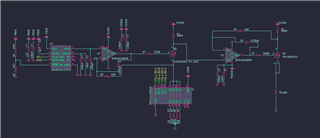
I created a design based on TIPD102 https://www.ti.com/tool/TIPD102#3. For the most part it is working great.
Unlike the original design, which has current between 0-100mA. My design requires much lower current with high precision 0-1mA, with emphasis on 100nA, 300nA, 1uA, 3uA, 10uA
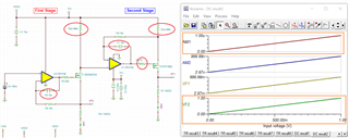
In the TINA-TI simulation (attached), the design seems to be working as expected. But in practice at 100nA and 300nA levels, I am seeing fluctuations in current bigger than what is desired.
For example, at 100nA I see the current fluctuating between 98nA and 102nA.
Design changes:
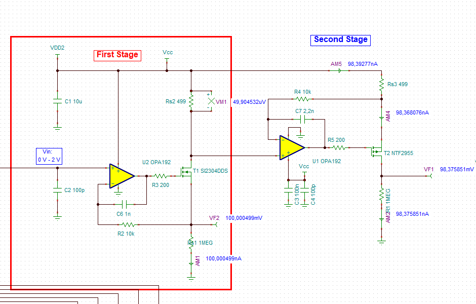
The relevant schematic of my design is shown below.
I am not completely sure where to start the debugging process and how to reduce this fluctuation, any feedback highly appreciated. I did some voltage measurements and the output from DAC seems stable.
Thank you,
This has to do with the input offset voltage of U1. The voltage drop across RS2 is in the same range as the input offset voltage of U1. Increasing RS2 results in a bigger voltage drop across RS2 and the input offset voltage of U1 plays a minor role.
Kai
Hi LazyHD,
I am not completely sure where to start the debugging process and how to reduce this fluctuation, any feedback highly appreciated.
Generally, you need first stabilize the V-to-I stage feedback loop first in the first stage. The second stage is current mirror duplication stage. Since the first stage is not stable, the second current stage will duplicate the constant current source at the first stage.
I made some modification in the circuit below. It should work for generating constant current from 100nA to 10uA. There are some circuit compensation issues.
1. The op amp V-to-I feedback is not stable (not enough phase margin). That may be why your the output current is not stable.
2. The op amp input on the secondary stage is too close to the 15V rail (but it was ok in complying with Vcm mode of OPA192). I placed 500k instead of 499 ohm.
3. The input stage in generating current is more accurate than the 2nd stage. I would use the output current at the first stage, unless you are driving something after the 2nd stage.
current-source E2E 08272021.TSC
There may be a better design approach for the low constant current application, but the circuit seems to be working in simulation.
Enclosed are some application notes for your future reference.
If you have additional questions, please let me know.
Best,
Raymond
That is thorough, thanks a lot for the suggestion. I highly appreciate it.
I will change the values on the board based on your suggestion and give it a try.
Please also note figures 13 and 14 of datasheet of OPA192 and what is written in section 8.3.6.
Kai
Hi LazyHD,
I am going to close this inquiry. If you have additional questions, you may still open the thread.
Best,
Raymond