This thread has been locked.

If you have a related question, please click the "Ask a related question" button in the top right corner. The newly created question will be automatically linked to this question.

INA826: Test method of PSRR

Part Number: INA826
Other Parts Discussed in Thread: OPA333, INA333

Hello TI experts,

My customer now tests INA826 for their new product.

in this step they want to know the test method of PSRR of INA826 for certain reason.

could you guide me about it? (including test equipment, connecting method, input condition, etc)

it will be very helpful for my customer.

Best regards,

Chase

  • Hi Chase,

    could you guide me about it? (including test equipment, connecting method, input condition, etc.

    Here is what you need.

    1. You need dual high quality linear power supplies.

    2. A function generator and scope.

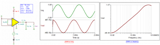
    3. Connect the setup as shown below. You need configure INA826 in a linear operating region. In this case, Vcm = 0 V

    4. Inject AC signal onto the Vcc or Vee rail, say 1kHz with amplitude 1Vp or another other frequency of interest (Injected AC is riding on the DC supply rail). 

    5.  Measure the INA826 output's amplitude at the injected frequency, where we are only interested in AC injected signal that is seen at the output. 

    6. Ratio Vinj/Vout, take a log of the ratio and multiple by 20 in PSRR = 20log(Vinj/Vout)

    7. In the example below, PSRR (RTO) = 20log(1V/487.7uV) = 66.24 dB at 1kHz + Gain = 100V/V, which is the same as the PSRR vs. frequency plot at 1kHz or 66.237 dB.

    8. RTO means Refer to Output, the datasheet is plotted in RTI or refer to input. 

    9. So you have to divide 487.7uV/100 = 4.877uV, which is 106.24 dB at Gain = 100 V/V and 1kHz --> this matches the plot shown in Figure 21.

    INA826 PSRR 08272021.TSC

    Note: Regarding sign issue, the PSRR definition is -20log(Vout/Vinj). If you do Vout/Vinj as shown in AC analysis plot, then you need to place a "-" sign in front of it the match the datasheet.  Also, you prefer to have  higher gain configuration in instrumentation amplifier, which CMRR and  PSRR will improve as gain increases. 

    If you additional questions, please let me know. 

    Best,

    Raymond

  • Hi Chase,

    it's important that both supply voltages are synchronously excitated, but 180° phase shifted to each other. Otherwise the measurement is flawed by the finite common mode rejection (CMRR) of INA.

    You might want to look into this thread:

    https://e2e.ti.com/support/amplifiers-group/amplifiers/f/amplifiers-forum/1014334/opa2836-how-to-measure-psrr-by-using-an-oscilloscope

    Kai

  • Hi Raymond, kai,

    Thank you for your support.

    I am very sorry that i had a typo, customer wants to know the test about CMRR, not PSRR.

    I think you already understand and guided me about CMRR, but please just confirm it once again.

    Best regards,

    Chase

  • Hi Chase, 

     Q: guided me about CMRR, but please just confirm it once again.

    Below is a TI video that reveals the CMRR test procedures, also see the attached simulation. 

    www.youtube.com/watch

    INA826 CMRR 08312021.TSC

    If you have additional questions, please let us know. 

    Best,

    Raymond

  • Hi Raymond,

    here are some more questions from my customer.

    1. if we use 2 INA826 in series, Does CMRR value increase or decrease?

    2. I saw figure 19 in datasheet below;

    It only represents that Vs=+/-15V. How about the case under Vs=+/-2.5V? Does CMRR value change under this condition?

    3. I also saw that REF pin must be driven by low impedance (in pin description)

    here is the schematic of the customer below. could you suggest something for REF pin driven by low impedance?

    please let me know if you need more information about this. Thanks.

    Best regards,

    Chase

  • Hi Chase,

    the common mode rejection of two INA826 in series? This sounds confusing. Can you show how they are put in series?

    With every additional OPAmp in the signal chain the common mode rejection will further detoriate. But the highest degradation can usually be seen in the stage with the highest gain, which usually is the first stage. But what really happens depends on the used parts and especially on the used circuit. Degrading the balance at the input of circuit can totally ruin the common mode rejection, for instance. But to give a correct answer one would need to see the full schematic.

    The REF pin can be driven by the low ohmic output of an OPAmp or by voltage reference chip, as shown in figure 61 of datasheet. The datasheet is full of examples.

    And the common mode rejection does not alter much, provided you stay well within the recommended supply voltage range.

    Kai

  • Hi Kai,

    thank you for your reply.

    I understand clearly question 1 for your kind description.

    how about Q2 and Q3? could you guide me more about it?

    Best regards,

    Chase

  • Hi Chase,

    Q: It only represents that Vs=+/-15V. How about the case under Vs=+/-2.5V? Does CMRR value change under this condition?

    I simulated CMRR (RTI) in Figure 19 with Vs = ±15Vdc and Vs = ±2.5Vdc per your request. Both plots are near identical, please find the attached simulation. 

    INA826 CMRR Different Vs 09022021.TSC

    3. I also saw that REF pin must be driven by low impedance (in pin description)

    This is an example of low impedance node for Vref pin in INA826. The image is captured from INA333's datasheet. The Vref pin is required to be able to source and sink, the output of OPA333 buffer is a low impedance node. 

    If you have additional questions, please let us know. 

    Best,

    Raymond