This thread has been locked.

If you have a related question, please click the "Ask a related question" button in the top right corner. The newly created question will be automatically linked to this question.

INA233: Is it calibrate the oA ?

Part Number: INA233


Hi,

We use 4 INA233 on a same board to measure output current and voltage, it's like a power distributor:  1 to 4 outputs

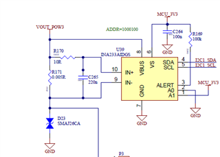
The layout of the first three INA233 is the same: The Rsense resistor and the INA233 are on Top.

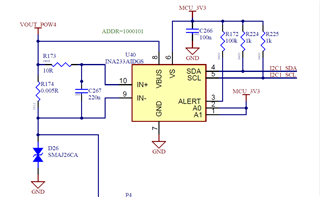
But the layout of the fourth INA233 is slightly, different : the Rsense resistor is on TOP and the INA233 is on Bottom.

The INA233 registers configuration is the same for all : ADC conversion time = 1.1ms & MFR_CALIBRATION = 4194 (MAX AMP= 8A) & Rsense = 5mOhms.

If the Vbus voltage is 0V, the 3 first INA233 measure about 2-3mA but the fourth measure about 9mA; I checked with several boards and the current measure of the fourth is always different of the first three.

We tried with a ADC conversion time = 8.244ms and an average of 64 samples, but not change, there is always a difference with the fourth (9mA instead of 2-3mA).

We changed the MFR_CALIBRATION register in order to have 0mA when there is no voltage level as indicated in the datasheet : "to cancel the total system error"; But only the coefficent change not the offset.

So I would like to know if the fourth INA233 has a problem or not ? and I would like to know if we can calibrate the offset in order to have 0mA when there is not voltage level .

Thanks, 

Jerome

  • Hey Jerome,

    I am looking into this question now and will respond shortly.

    best,

    Peter

  • Hey Jerome,

    Would please shows images of the differing schematics? I am not sure what you are describing.

    What you describe about adjusting the calibration register value based upon system calibration makes sense. The process as described in section 7.5.5 only calibrates for gain error, not offset error, so this is why the coefficient changed, but not the offset.

    What is the point of R713? Could you repeat this test, but shorting out R713?

    9mA offset does seem high, although given R713 it is not impossible, especially if there is some layout issue here. The input bias current when input is a 0-V could fluctuate if the input voltage is not really being pulled low to ground, but rather being floated or being pulled to ground with high resistance. For many device the IB can go negative (current coming out of device). To get 9mA offset reported, all that is needed is ~+46µV input offset. If IB+ = -3µA, then a worst-case offset can become:

    Vos_max = Vosi + Vos_cmrr + Vos_IB+ 

    Vos_max = +10µV + |12-0V|*10^(-126dB/20) - (-3µA*10Ω)

    Vos_max = 10 + 6 + 30µV = 46µV --> +9.2mA = 46µV/5mΩ offset reported

    I would try shorting out R713 as I don't see a purpose for it and see if the error continues. If it is still there, there could be a layout discrepancy or a input voltage discrepancy. Please provide images of layout and the differences between the four circuits.

    Sincerely,

    Peter

  • Hi,

    There is no schematic difference, e.g CH 4 & CH3:

  • But there is a difference  about layout : 

    CH4 : U40, R173 in BOTTOM  & R174 in TOP + Nets of IN+ & IN- are routed TOP and Bottom

    CH3 : U39, R171 & R170 are placed in TOP + Nets of IN+ & IN- are routed TOP and Bottom

  • I did test with R173 and with R173 shorting, the output  is pulled low to GND:

    R173 = 10Ohms, the INA233 measures 7mA

    R173 = shorting, the INA233 measures 11mA

    => with R173 shorted, the error is higher.

    Thanks

  • Hey Jerome,

    So it makes sense that offset got worse when shorting R173. The reason is because input filter offset (due to the R174) is going to be negative because the IN+ input bias current (IBP) can be negative (going out of IN+ pin) when VCM = 0V. All it takes is IBP = -2µA, in order to generate a delta of -4mA of input offset.

    What does not make sense is how the offset is already so high with channel 4. There are definitely some things that can be improved with the layout of input traces for both channels shown and you can refer to my modified layout example from datasheet. Overall, it is best practice to route the traces through the pads of the 220nF input capacitor (i.e., C267, C265). In your current layout the input traces go directly to the input pin and not through the capacitor pads.

    The layout suggestion above doesn’t seem to be the real root cause here, but I though I would mention anyway. However, there seems to be a trace from the shunt-side of the 10-Ω (i.e., R173 for ch4 and R170 for ch3) that goes outside of the image. Where do these traces go? See the below images with the trace marked with green markup.


    Sincerely,

    Peter

  • Hi Peter, 

    This trace is for a "Power Line Communication" :  the data is phase modulated by a sine wave at a predefined carrier frequency -@10,4MhZ).

    e.g : PLC output : C is 2n2F in our schematic

    I did test without C (2n2F) and with the PLC component in a RESET mode, but the offset current measured doesn't change.

    Thanks,

    Jerome

  • Hey Jerome,

    How many systems are showing this behavior (channels 1-3 are good, with channel 4 offset high)?

    Could you make sure the board have been cleaned with no flux residue left behind and re test?

    Did you do this test (without the 2.2nF) on the problematic channel 4 of a board showing the high offset? Or was that a with channel showing the 2-3mA offset?

    After confirming that this capacitor nor unclean boards are not causing any leakage on channel 4, I would suggest making some some voltage measurements across the 10-Ohm input resistors for all four channels. Measurements of the supply voltage (Vs pin to GND pin), across the shunt resistor, and directly at the input pins of the INA233 (voltage from IN+ pin to IN- pin) would be good too. A common mode voltage at input (IN+ to device GND pin) will also be good.

    After taking these measurements, try swapping the device from channel 4 (high offset) from another channel showing normal offset. Re test the system offset with no load current and see if the problem follows the device.

    Sincerely,

    Peter

  • Hi Peter,

    I plan to do few measure like you said, but I am not free time to do it now.

    I hope to do it in 2 weeks.

    Sorry,

    Jerome

  • Hey Jerome,

    No problem. I look forward to your updates then. 

    Sincerely,

    Peter

  • HI Peter, 

    How many systems are showing this behavior (channels 1-3 are good, with channel 4 offset high) ? Yes channel 1, 2 & 3 are good and the channel n°4 has an high offset; There are four channels by PCBA (board), and i have the same behavior (high offset on channel n°4) on all my PCBA (more than 20 PCBA)

    Could you make sure the board have been cleaned with no flux residue left behind and re test?I think that the board have been cleaned with no flux residue, I will ask to my EMS.

    Did you do this test (without the 2.2nF) on the problematic channel 4 of a board showing the high offset? Yes I test with and without 2,2nF (channel n°4)

    Or was that a with channel showing the 2-3mA offset? I test with 2,2nF (Channel n°1,2,3)

  • After taking these measurements, try swapping the device from channel 4 (high offset) from another channel showing normal offset. Re test the system offset with no load current and see if the problem follows the device.

    Before change, the INA233 of CH4 measures 8mA ,

    After changed (component mounted on CH n°1 and then mounted on CH n°4), the new INA233 of CH4 measures 6,1mA,

    Thanks, 

    Jerome

  • Hey Jerome,

    I apologize for the delay. I was out of the office.

    Was R173 populated when you did this test? Let the INA233 from CH4 measuring 8mA be called NG1. Can you move the NG1 to channel 1 and record the measurement? 

    Alternatively, what did the original unit from Ch1 measure for its offset before moving to channel 4?

    Overall all of the input 10-Ohm resistor should be shorted out in addition to the layout recommendations I provided earlier.

    Sincerely,

    Peter

  • Hi,

    Yes R173 was populated.

    I tried to move NG1 to channel 1, but I damaged it in soldering.

    The original measure from CH1 was -0,9mA.

    About  Overall all of the input 10-Ohm resistor should be shorted out, you said before : So it makes sense that offset got worse when shorting R173.

    Thanks,

  • Hey Jerome,

    Well it seems like the discrepancy and large offset is due to some difference in layout. I would recommend to try isolating the physical layout differences between channels to see what is causing the offset. One example could be disconnecting the PLC trace from the INA233 input pin.

    I would also make there is no flux residue near channel 4 or along its corresponding PLC trace to make there is no leakage current occurring at channel 4 input traces.

    Sincerely,

    Peter