
- Ask a related questionWhat is a related question?A related question is a question created from another question. When the related question is created, it will be automatically linked to the original question.
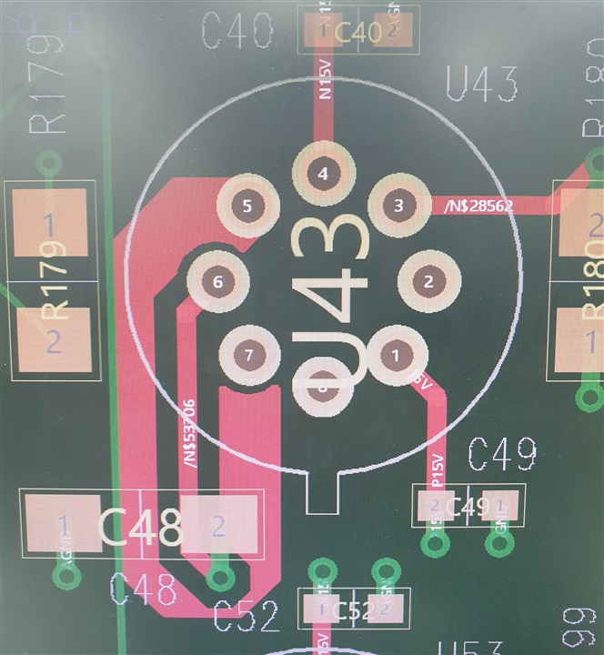
Above the picture, the Green pattern is located on the PCB TOP Layer, and the Red pattern is located on the PCB Bottom layer, which makes them look overlapped with each other.
U43 is an LF198 (Sample & Hold) chip, pin(5) is an output pin, pin(6) is a hold cap pin, and C48 is a Hold capacitor.
I'm going to design the Guard Ring for the Sample & Hold chip, but is it problem when applying the Guard Ring as shown in the picture above??
If it is a wrong Guard Ring pattern design, Please check how the guard ring should be applied.
Thanks
best regards.


