This thread has been locked.

If you have a related question, please click the "Ask a related question" button in the top right corner. The newly created question will be automatically linked to this question.

OPA818: Testing TIA with VNA

Part Number: OPA818
Other Parts Discussed in Thread: OPA855

Hello,

I had asked on this topic before, unfortunately it seems I am not able to make this measurement successfully. I have a TIA with 5kohm gain that connects to a bare die with a high speed photodiode (which is bonded to the pcb). We have the desired signal around 1-50 MHz. According to the PD manufacturer, the diode should have sub pF capacitance and since we only need maximum 50 MHz, we added a 33pF C to limit the bandwidth.

The big yellow block on the left would contain the photodiode, and closes the loop. In our test board, we don't have the photodiode yet and we close the loop on the PD Bonding PCB via a 0 ohm resistor. Since the capacitance of the diode should be small compared to the 33pF we have on the inverting input of the 818, I was hoping we could test the circuit without it. Unfortunately, I am not able to get good agreement to the transimpedance gain I expect (5k) ~ 74 dB. We have MMCX connectors so have clean transition to our VNA cables. We chose 1nF and 4pF for the "current divider caps" and matched input and output to 50 ohm.

The s-params look as follows:
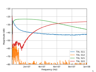
Can anyone provide some guidance on how we can get back to the transimpedance curve from this?

Any help would be greatly appreciated!

best regards

Dominik

  • Hello Dominik,

    I am going to read through the previous post Sima & Michael assisted you with, as well as look over your information in this post.

    Please give me some time to review this information and get back to you in a reasonable manner.

    Best,

    Alec

  • Hi Dominik,

    putting so many components into the feedback loop is counterproductive, as every component and the associated copper traces add unwanted parasitic inductances and stray capacitances. When you work with a decompensated 2.7GHz OPAmp you should limit the number of components in the feedback loop to absolute minimum.

    This is also valid for the VNA circuit. With all the additional components you change the original circuit so much, that you will not be able to measure the true performance of TIA. So, I would give up the VNA circuit, but would keep the circuit as simple as possible and just trust the simulations. There's hardly more you can do.

    I would go for this circuit:

    dominik_opa818.TSC

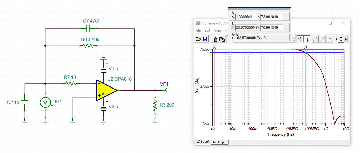
    Allow a bit headroom for the bandwidth to take into account component tolerances and parasitic impedances. I have chosen 84MHz instead of 50MHz. Put only one 4k99 resistor and one 0.47p cap into the feedback loop and no more components. Remember, the OPA818 is a 2.7GHz OPAmp, no 2.7MHz. Frequency response and pulse response are perfect and the phase stability analysis shows an awesome phase margin of 60°.

    dominik_opa818_1.TSC

    What more do you want?

    Kai

  • Hi ,

    Thank you for your recommendation and the circuit example! I understand where you are coming from (limiting the number of components etc), but unfortunately, we need a means of saying this circuit is working before we place the diode on the pcb. We are working with unpackaged components here in collaboration with another company. The process is highly volatile on their end, so the coupling loss from the diode could be quite high. We need to be able to provide at least some indication that our circuit is working before we transfer the pcb to them for glueing and bonding of the diode. That way, if the end result doesn't work, we can more easily troubleshoot and avoid the blame game :) We can disconnect this test circuit physically after verification by removing the series cap, assuming that we can show in simulation that it does not alter the behavior of the circuit significantly. I think we are quite close with the existing setup, the 3dB point is right where it should be, likely thanks to the massive 33pF shunt capacitor which is dominating the additional parasitics. The only thing missing is converting this S21 back to the actual transimpedance gain.

  • Hi Dominik,

    in your scheme is a mistake:

    C10 must be equal to the detector capacitance, which is sub-Picofarad, as you mentioned. Increasing C10 to 4pF turns the circuit into a totally different circuit.

    More, I would increase C4. To decrease the parasitic inductance of C4, put several identical caps in parallel.

    And keep in mind, that too many millimeters of copper traces at the -input of OPA818 can totally alter the circuit. So put C10 and C4 closest to the input of OPA818.

    I'm still not convinced, that having the cap-T and the huge 33pF in your circuit is a good decision. Believe me, when it comes to GHz OPAmps "less is more" Relaxed

    Kai

  • Hi Kai,

    I believe you :) - but my problems stands. There must be a way to test this 50 MHz circuit that provides some confidence of "everything appears to be working" (no solder problems, tombstone C's, etc). If the measured gain deviates from the "real" circuit by 5-10%: fine. If the fc is pushed in or out 10%: also fine! I just need proof that the circuit/pcb is working before it is shipped to our partner. As per the 50 Ohm resistor, I agree, in the schematic with 1nF C4, this would provide a terrible match. The purpose of the DNP was to expand the shunt capacitance, Ideally to 100nF. I fear the parasitic L will ruin our day though. If we could have 100nF then the series 50 ohm would again provide a nice match through C4 to ground. Once I'm back in the office I can try a 100nF at C4 but I think I did this already and it caused significant peaking.

    Thoughts?

  • Hey Dominik, your request is very common - here is the original article talking about this, 

    Here's an easy way to test Zt article steffes 1998.pdf

    Here I modified Kai's file to produce the input signal. Using very low L X2Y cap (johannson) for the shunt C gives a flat input stimulus from about 2MHz to over 100MHz - greatly attenuated. So this is your input signal using this technique - pretty small current but so is the actual signal,

    Looking at the amp output shows this expected gain - and this would likely go out through 50ohm to a VNA 50ohm sense path, so yes, if you can measure this the circuit is likely working - I went ahead and added the bias current cancellation on the V+ input - not needed for JFET input - normally with Zt gains <200k we would use a bipolar input op amp like the OPA855, 

  • I should have looked at my article, forgot the series 50ohm termination into the cap divider - those caps go short circuit so that 2nd series 50ohm drives its current into the two caps looking like an ok match. I also set up the output network into the VNA, 

  • Hi Dominik,

    it should be noted that it is not so much the inductance of C4 which ruins the performance of this circuit but the unavaoidable self resonance of C4:

    dominik_opa818_2.TSC

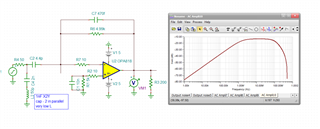
    Above you see a simulation where the inductance ("L1") runs from 1pH to 1nH. See how the self resonance frequency wanders down when the inductance increases. 318MHz for 250pH, 230MHz for 500pH and 160MHz for 1nH. So if you want to verify the 84MHz corner frequency of the original circuit (see my earlier simulations), the self resonance frequency should be considerably higher than 84MHz.

    What does this mean for you?

    1. You should not increase C4 too much. 100nF will definitely be too much. Better stay in the nF range.

    2. Keep the inductance of C4 as small as possible. 0402 package for C4 is way better than 0805 or 1206. Paralleling can help, but only if the caps are referenced to a solid ground plane and are sitting close together. "Sandwiching" can be a remedy. Or take X2Y caps as recommended by Michael. Unfortunately most X2Y caps come with high manufacturing tolerances.

    3. The frequency response above the self resonance frequency of C4 obviously shows nonsense and is dominated by the parasitics behaviour. You cannot use this frequency range to check whether your circuit is running properly or not.

    There's another point. You can increase R4. This will flaten the curve at lower frequencies by introducing a lower corner frequency of high pass filtering. See the curve above. But increasing R4 by a factor of ten will decrease the output signal by a factor of ten as well:

    Kai

  • That is true, the X2Y are +/-20% tolerance but what you are really after is that 50pH inductance to hold the injected current signal flat through 100MHz. The cap tolerance

    1. changes where the injected current goes flat at lower F, kind of a don't care as long as it it is well below the higher F cutoff you are trying to measure. 

    2. Changes the apparent midrange gain to the output as you get a variation in the current divider at the input - well that midband gain is what you are after to measure the F-3dB from that - a relative measure, not absolute - variation there can be attributed to the cap tolerance and ignored. 

    I vaguely recall trying to get Johansson to provide tighter tolerance X2Y so I could use them in ADC final stage filtering - with no luck. I think there must be low L RF caps out there also the would be useful in this test application. 

    https://www.johansondielectrics.com/downloads/x2y-filter-and-decoupling-capacitors.pdf

  • Hello Dominik,

      Sorry that I missed your additional reply in the original older thread. For that reply, I believe you found out the higher bandwidth would be limited by the following TIA with cutoff frequency set by feedback components + input capacitance. The parallel capacitance as Kai and Michael have answered already are for reducing parasitic inductance. When implementing the photodiode path, you wouldn't have to worry about this, but rather the parasitic of the trace which can be avoided by placing the photodiode as close to the input pins of the amplifier as possible.

      Using Michael's method and Kai's Tina simulation, try this circuit configuration (with removal of any components on the other path such as 33pF and 10Ohms at the input of the amplifier): (Kai's circuit in earlier reply has varying parasitic inductance which is very useful) 

        If you would need to further limit the bandwidth, I would suggest a passive filter at output of the TIA, or choosing a lower GBW amplifier. (2pF accounting for sub-pF photodiode capacitance and internal input capacitance of the amplifier).  

      TIA calculator can be found at this link, and here is also a link with filtered list of other amplifiers. With this low of feedback resistance, bipolar input amplifier might be a better option noise-wise. 

    2502.dominik_opa818_2.TSC

    Thank you,

    Sima