Other Parts Discussed in Thread: OPA858
Hi there,
I was hoping to get help with the OPA858 amplifier.
Initially it was included in the PCB layout to be used as a Transimpedance amplifier, but now there is a plan to use it as a voltage amplifier-assuming it can do the job so to speak.
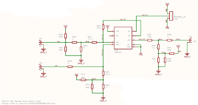
Figure 1, is the layout on our PCB, it is more or less similar to that of the evaluation board. When testing it as a TIA, it demonstrates a power loss of roughly 35 dBm (using a spectrum analyzer). It was initially a little over 40 dBm loss, but there were a few minor adjustments that were made including using newer SMA cables as well as shrinking the size of the SMA connector pad (it was initially too wide).
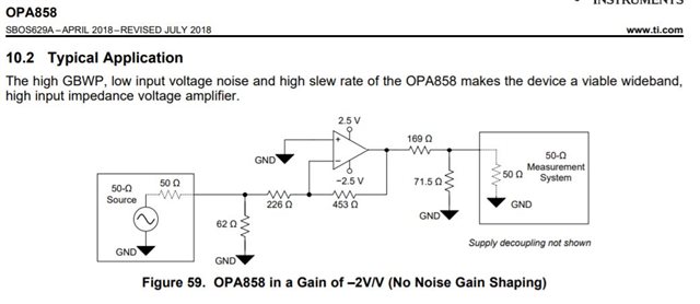
Figure 2 is taken from page 22 of the OPA858 datasheet in which it illustrates how it can be used as a voltage amplifier. I am currently using this layout (figure 59 in the screenshot) and the power loss experienced is approximately 30dBm.
I then incorporated an oscilloscope with the testing in order to see the power loss/gain illustrated as a sine graph. In this scenario, the signal attenuates from 700mv pkpk --> 75mv pkpk. When I increase the input voltage (voltage source to the PCB from +/- 1.6v to 2.6:dual supply) that signal will amplify from 70 mv pkpk to 240 mv pkpk.
So technically there is amplification, but only after experiencing overwhelming attenuation.
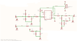
Figure 1
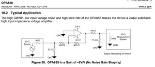
Figure 2
I have multiple of the same PCB boards and then tested the voltage amplifier configuration on a second board. The power loss when testing using the Spectrum Analyzer is around 45 dBm. When using the oscilloscope the initial attenuation is still the same (700mv pkpk to 70 mv pkpk) but amplification is no longer possible.
Essentially I was hoping that you would be able to aid in resolving this problem. There is obviously a problem with figure 1 (our original layout), I was wondering if you would be able to help out in that case. We did have the evaluation board which worked as expected, unfortunately during testing, one of the technicians accidentally burnt the OPA858 chip- so it will take some time before we can replace that board.
Thank you very much
Best regards,
Tayeb