- Ask a related questionWhat is a related question?A related question is a question created from another question. When the related question is created, it will be automatically linked to the original question.
This thread has been locked.
If you have a related question, please click the "Ask a related question" button in the top right corner. The newly created question will be automatically linked to this question.
Hi there,
I was hoping to get help with the OPA858 amplifier.
Initially it was included in the PCB layout to be used as a Transimpedance amplifier, but now there is a plan to use it as a voltage amplifier-assuming it can do the job so to speak.
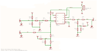
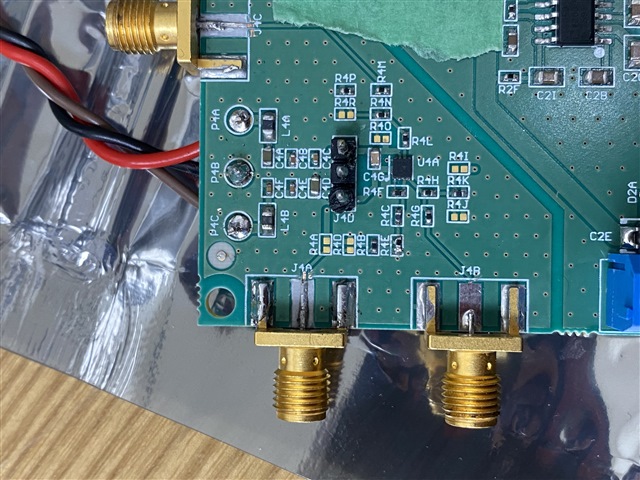
Figure 1, is the layout on our PCB, it is more or less similar to that of the evaluation board. When testing it as a TIA, it demonstrates a power loss of roughly 35 dBm (using a spectrum analyzer). It was initially a little over 40 dBm loss, but there were a few minor adjustments that were made including using newer SMA cables as well as shrinking the size of the SMA connector pad (it was initially too wide).
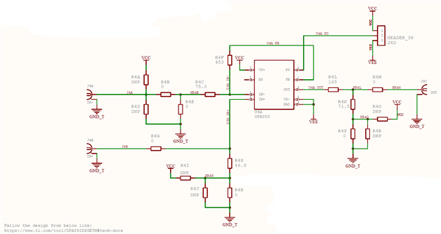
Figure 2 is taken from page 22 of the OPA858 datasheet in which it illustrates how it can be used as a voltage amplifier. I am currently using this layout (figure 59 in the screenshot) and the power loss experienced is approximately 30dBm.
I then incorporated an oscilloscope with the testing in order to see the power loss/gain illustrated as a sine graph. In this scenario, the signal attenuates from 700mv pkpk --> 75mv pkpk. When I increase the input voltage (voltage source to the PCB from +/- 1.6v to 2.6:dual supply) that signal will amplify from 70 mv pkpk to 240 mv pkpk.
So technically there is amplification, but only after experiencing overwhelming attenuation.

Figure 1
Figure 2
I have multiple of the same PCB boards and then tested the voltage amplifier configuration on a second board. The power loss when testing using the Spectrum Analyzer is around 45 dBm. When using the oscilloscope the initial attenuation is still the same (700mv pkpk to 70 mv pkpk) but amplification is no longer possible.
Essentially I was hoping that you would be able to aid in resolving this problem. There is obviously a problem with figure 1 (our original layout), I was wondering if you would be able to help out in that case. We did have the evaluation board which worked as expected, unfortunately during testing, one of the technicians accidentally burnt the OPA858 chip- so it will take some time before we can replace that board.
Thank you very much
Best regards,
Tayeb
Input from Spectrum Analyzer: 100 kHz & 3 dBm (1.5413 V pkpk on oscilloscope) All Measurements noted are pkpk
Measurements: Voltage Amp configuration (PCB not powered on)
---------Pre OPA858---------
J4A (SMA input): 1.5413 V R4E (75ohms): 1.5413 V R4C (220ohms): 1.5413V
--------------------OPA858---------------------------
Pin FB: 415mV Pin PD: 59mV
Pin NC: 59mV Pin +VS: 59mV
Pin -IN: 1.16V Pin OUT: 415mV
Pin +IN: 59mV Pin -VS: 59mV
---------------------------------------------------------
-------Post OPA858-------
R4L (169ohms): 138mV
J4C (SMA output): 140mV
--------------------------------------------------------------------------------------------------------------------------------
Input from Spectrum Analyzer: 100 kHz & 3 dBm (1.5413 V pkpk on oscilloscope)
Measurements: Voltage Amp configuration (PCB powered on)
---------Pre OPA858---------
J4A (SMA input): 1.44 V R4E (75ohms): 1.44 V R4C (220ohms): 1.44 V
--------------------OPA858---------------------------
Pin FB: 60mV Pin PD: 60mV
Pin NC: 59mV Pin +VS: 60mV
Pin -IN: 553V Pin OUT: 69mV
Pin +IN: 277mV Pin -VS: 0mV
---------------------------------------------------------
-------Post OPA858-------
R4L (169ohms): 38mV
J4C (SMA output): 40mV
I realize that I have not yet made the changes that you mentioned above, but I wanted to illustrate that from what I can tell, the attenuation is taking place prior to the the OPA858 chip itself and seemingly because of the chip itself. I have highlighted in the red font, the inputs and outputs to the amplifier chip itself and it is evident that there is roughly an attenuation of 30% when the PCB is not powered on and almost 8x attenuation when it is powered on.
I am hoping that this additional information can help in diagnosing the problem.
I would think that the problem would be with the OPA858 chip itself, but the problem is present in more than one board and though not impossible, it seems unlikely that problem is with the chip in question.
I will attempt to make the requisite changes you mentioned in your response, but if it's possible, I would appreciate it if you could look over the data I have included above.
Thank you once again,
Tayeb
Hi Tayeb,
it's a bit confusing to me. Can you show a schematic which exactly contains the populated components?
Kai
Figure 1 that I included in the first post is the schematic I am testing. It was meant to be a Transimpedance amplifier, so I made the 2 changes from Figure 59 on page 22 of the datasheet to use the OPA858 as a voltage amplifier.
Changes to figure 1: R4E --> 62 ohms (75 in my case) and RFC -->226 ohms (220 in my case).
So its essentially figure 1 with the above to changes.

The SMA pads were altered after the fact as the pad was too wide for the connector (hence the rough finish).
The amplifier outputs only a DC voltage, there does not seem to be any AC voltage after the amplifier, I have run it from various frequency ranging from 20 kHz to 100 MHz, the lack of AC output voltage continues.
As odd as this may seem, please disregard the output values (values after the OPA858 I included in the post before this) though there is attenuation, the values were read incorrectly.
Hi Tayeb,
giving a signal to the input of OPA858 while the OPAmp is unpowered is no good idea at all. By this you violate the absolute maximum ratings (see section 7.1 of datasheet) and risk a destruction of OPA858. Very probably you have already destroyed the OPA858 by this torture.
If you cannot guarantee that the OPA858 is powered before an input signal is applied, use a HF-relay which disconnects the input signal as long as the supply voltage of OPA858 is down.
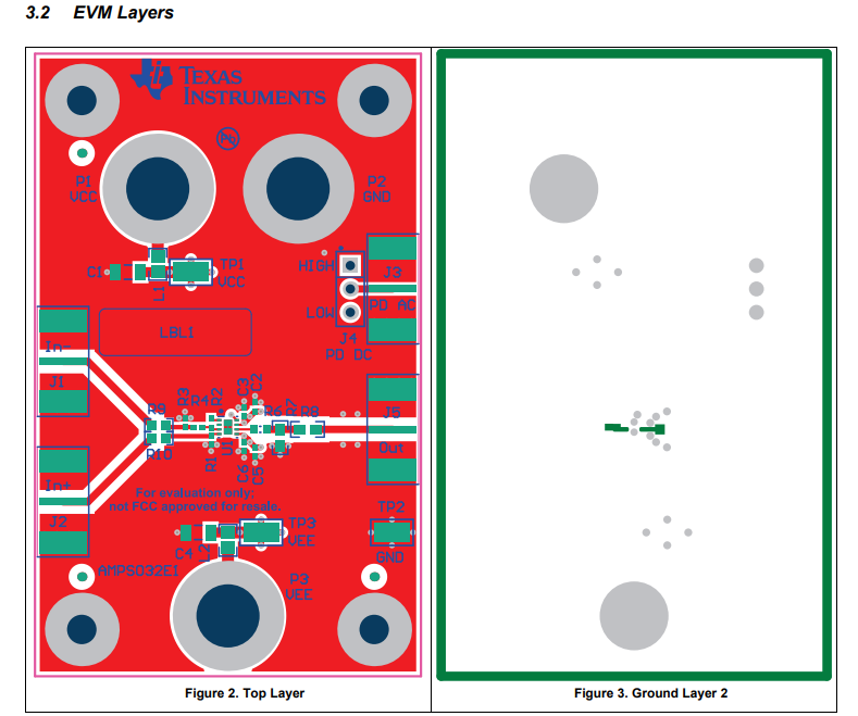
Also, your layout is not suited for a decompensated 5.5GHz. Keep in mind that the OPA858 is no 5.5MHz OPAmp but 5.5GHz. This is 1000 times faster! Compare your layout with the recommended layout from the EVM and you will see what I mean:

Reduce the length of copper traces of gain setting components to the absolute minimum. Every millimeter counts. And reduce the number of gain setting components to the absolute minimum. You cannot make an "all-purpose" layout in this way with the OPA858. By having so many components in the signal chain you add so much additional parasitic inductance and stray capacitance that the circuit can even become unstable.
Kai
We have 2 boards, #1 and #2.
Board #1--> I inputted a signal before powering on the PCB-admittedly the signal strength was 1.5pkpk which according to the datasheet is outside the limit.
Board #2--> has not been tested without powering on the PCB
--------------------------------------------------------------------------
Board #1, when powered on via dual power supply @ +-2.2V with 200mv pkpk input signal, only has a DC output of -900mv after R4L-->169ohm out resistor
Board #2, when powered on via dual power supply @ +-2.2V with 200mv pkpk input signal, only has a DC output of 40mv after R4L-->169ohm out resistor
--Only one of the above boards was 'tortured' yet they both have only DC outputs
Hello Tayeb,
It looks like power-down pin is driven low, which would set the amplifier to power off mode. Setting this pin to logic high will put the amplifier in normal operation. Hopefully, this might fix the issue:
I do agree with Kai's assessment and suggestion on layout, and concern with violating the abs max rating of the part by applying an input voltage to an unpowered amplifier. These high bandwidth parts unfortunately need a dedicated high speed layout to avoid signal oscillations. I have attached the Gerber files and the 3d step file for the OPA858EVM below that you can use to follow.
7206.AMPS032E1_GerberNCdrills.zip
Thank you,
Sima