This thread has been locked.

If you have a related question, please click the "Ask a related question" button in the top right corner. The newly created question will be automatically linked to this question.

THS3491: Post-Design question

Part Number: THS3491
Other Parts Discussed in Thread: DAC3154, THS3217,

Hello,

I have designed the post-DAC amplifier from good ideas mentioned on this forum.

The input to this stage is driven directly from current output DAC3154.

The board is up and running, and seems to work OK.

However I would like feedback on the design. Any comments or suggestions for improvement will be appreciated and I will incorporate into any next spin.

Thanks

Daviddac_amp.pdf

  • Hello David,

      Thank you for taking note of Michael's previous suggestions for this project. 

      Another TIer will get to reviewing the design. In the meantime, I did look through it myself, and a few questions:

    1. Would you be able to provide the layout of your board. You can share it to us privately via email if you would like: s-jalaleddine@ti.com 
    2. Are you looking to add higher order filter between stages? What is your frequency range, is it still around 100MHz?
    3. I would suggest maybe adding testpoints/connectors to mid and reference pins on the THS3217 if you would need to apply level shifting or adjust the common mode voltage.

      Overall pretty good implementation of the isolation resistors and power supply filtering.

    Thank you,

    Sima 

  • Hi Sima

    I will send you layout privately (tomorrow - since at home today). Can you see BRD files or prefer PDF?

    The DAC sample frequency will be an absolute maximum of 200MSPS.

    Output frequencies in the range few MHz to 50MHz.

    At present no higher order filter.

    Will consider your idea of test-points - thanks.

    The devices are running pretty hot even though I did my best to heat sink them.

    I may consider removing the source termination (50 ohm) and running at lower voltages.

    Thanks

    David

  • Morning David, 

    Looks pretty good to me, I don't think we ever looked at disabling the OPS and putting no external resistors for it. Might be safer to add a 750 Rf feedback in and a 200 resistor to ground on the OPA V+ input. I think you have places for those, you might try that and see if the heat goes down - not likely an issue, just something to try. 

  • Michael,

    I will try it.

    Thanks

  • Hello David,

    Sima shared your emailed images with me; I am thinking through what could cause the devices to run so warm.  Could you confirm what your output voltage range is at the output of the THS3491?

    Best,

    Alec

  • Hi all,

    I finally bought an IR Thermal measurement tool and am reading 35-45 for the THS3217 / THS3419.

    I guess this is reasonable even though it is feeling hot to the touch.

    At some stage I will stick a real thermocouple and measure more accurately.

    The DAC on the other hand is running at about 60 C. I think there is room for improvement for DAC thermal dissipation in the next board spin.

    Regarding adding 750 and 200 around OPA V+,  I can do that in the next spin.

    The decoupling caps that Sima mentioned are on the PS, and yes, their connections to device and power could be improved.

    The output of the THS3491 is at 0V (unless of course I am sampling with the DAC).

    David

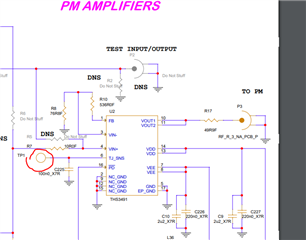
  • hey David, why don't you use the on chip temperature measurement port we put into the THS3491? It shows up in your schematic, 

  • Hi Michael,

    I guess the best answer to your question is "I just over looked the obvious".

    Using the sense I get junction temp (device output at 0V) is about 45C. (ambient about 20).

    I think I can live with this.

    Thanks for pointing this out.

    David