This thread has been locked.

If you have a related question, please click the "Ask a related question" button in the top right corner. The newly created question will be automatically linked to this question.

OPA320: Photodiode application slang

Part Number: OPA320
Other Parts Discussed in Thread: OPA392

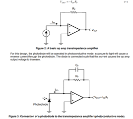
I was reviewing this 2014 reference design by Caldwell,\ (TIDU535),  I believe he misuses the "photo-conductive" term here - his circuit at this point is zero bias on the photo-diode which is commonly called photo-voltaic where Photo-conductive is used for reverse biased detectors, 
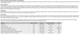
Here is one of many references that make this distinction, If I am missing something, and I have not gotten all the way through this Caldwell document, let me know. 

All About Photodiodes.docx

  • Also, there was this recent OPA392 thread using an OSI photo-voltaic detector.

    https://e2e.ti.com/support/amplifiers-group/amplifiers/f/amplifiers-forum/1078373/opa392-transimpedance-amplifier-for-photodiode-using-osi-optoelectronics-pin-10dpi-and-opa392?tisearch=e2e-sitesearch&keymatch=opa392#

    Small issue, but I was coming into this area (again) having the names reveresed in my own mind as well - part of that is there is some inconsistency out there with things like TIDU535. It is kind of confusing slang, one of the good articles on this thinks photo-voltaic is misleading, and should be called zero bias - I agree with that. True Photo-Voltaic detectors are a different world than true back biased photo-conductive detectors. Decades ago, I recall an HP book on photodiodes where the photo-voltaic mode was distinguished by running the reverse detected current into just a shunt R, producing a small voltage - that seems to have faded away, but the idea of generating a simple voltage in an R to ground might explain where that name came from. 

    It has not completely faded away if you check out these very specialized Thorlabs photovoltaic detectors - seems they are specified with just a shunt R? BUt its hard to tell, I got that as a technical reply to a question of sensor capacitance. 

    https://www.thorlabs.com/newgrouppage9.cfm?objectgroup_id=11319

  • Hi Michael,

    photovoltaic is when the photodiode is allowed to work like a solar cell, or by other words, when the anode of photodiode has a positive potential referring to the cathode, including the case that the voltage is zero (zero bias). Photoconductive is when the photodiode is not allowed to work like a solar cell, or by other words, when the anode of photodiode has a negative potential referring to the cathode.

    A photodiode is made from p-doped and n-doped semiconductor layers at the contacts. Space charge regions are forming within the pn-junction with a majority of electrons sitting in the p-doped contact layer and a majority of holes in the n-doped contact layer. As result a depletion area is forming with no electrons in the conduction band. And an electrical field "E" is forming by the space charge regions which is oppositely directed to the p-doped and n-doped layers.

    When a photon is hitting the depletion area, a free hole/electron pair is created. "Free" means that it is pushed from the valence band into the conduction band. Due to the internal, oppositely directed electrical field "E" the hole/electron pair is sorted and the holes are running to the p-doped anode and the electrons to the n-doped cathode. They both form the so called "photocurrent".

    When a load "R" is externally connected from the anode to the cathode of photodiode, a current (= photocurrent) is flowing out of the anode ("technical" current direction!), allowing the anode to develop a positive potential referring to the cathode, as consequence of the voltage drop across the load "R" caused by the photocurrent. ("Technical" current is assuming free positive charge carriers making the current flow.)

    This mechanism is called "photovoltaic effect", in opposition to "photoelectric effect", where the electrons are leaving the material being hit by the photons. Concretely, the photovoltaic effect means the creation of free charge carriers, being pushed from the valence band to the conduction band by photon energy. And in the photodiode they are even able to reach the contacts.

    The funny thing is, that the photocurrent mechanism is always the same whether the photodiode is operating in photovoltaic mode or photoconductive mode. The "motor" of the photocurrent is always the same internal, oppositely directed electrical field "E" which sorts the holes and electrones and makes them running to the opposite contacts. The only difference is the width of depletion area and the strength of electrical field "E" and the associated effects like junction capacitance, dark current, quantum efficiency, a.s.o.

    The current flow is only different, when you connect a high forward voltage from the anode to the cathode. Then the photodiode starts to behave like a simple diode with the forward current dominating the photocurrent. The forward current is flowing internally of photodiode from the anode to the cathode. But if only the photocurrent is flowing, it will always flow internally from the cathode to the anode. The current direction is identical to the current direction in a battery or accumulator then, where a chemical process creates an EMF and forcing an internal current to flow from the minus pole to the plus pole, which outside the battery flows from the plus pole back to the minus pole.

    It's interesting to note, that a photodiode being installed in a zero bias TIA, is indeed operating in photovoltaic mode. Not only because zero bias is per definition meaning the photovoltaic mode, but also, because due to the non-ideal, finite open loop gain of a real TIA the photodiode is (at least from theoretical point of view) always operating in forward direction. Of course, the forward voltage will be quasi zero in a good TIA. Also, the input offset voltage of TIA (and its input bias current) should not be forgotten, which usually dominates the required input voltage caused by the finite open loop gain of TIA.

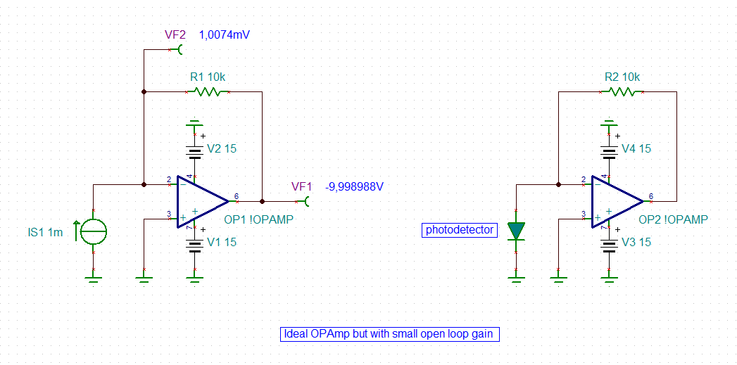
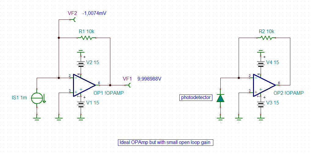
    In the following simulation an ideal OPAmp with zero input offset voltage and zero input bias currents but very non-ideally low open loop gain of 80dB is assumed to better demonstrate the effect of finite open loop gain on the polarization of zero biased photodiode in a TIA:

    michael_photodetector.TSC

    The left side and the right side show the same situation. For a better demonstration the photodiode is connected to make the TIA output a negative voltage. As you can see the photodiode is indeed connected in forward direction Relaxed

    Yes, I know it's improbable, but maybe this effect of finite open loop gain is the reason why the operation in a zero bias TIA is called photovoltaic mode? At least, it helps me to remember that zero biasing is called "photovoltaic mode".

    Kai

  • Thanks for all the detail Kai, way at the end you show the anode on the V- node of the op amp, yet all the diode manufacturers for photvoltaic show that reversed? 

  • Hi Michael,

    there's no big diffrence. The photodiode is still connected in forward direction:

    Kai

  • As soon as I sent that, I was thinking either polarity is probably ok with current coming out of the anode with this cathode on the op amp inverting input will give a positive going output voltage - which is what you want for a single supply implementation. 

    Thanks again for all the great detail Kai, unless someone else pipes up I am going to proceed with the assumption that that "photoconductive" labeling in Caldwell's reference design should have been photovoltaic due to the zero bias. Reading the vendor literature, the advantage of zero bias is no dark current, the disadvantage is much higher source C which pushes the required op amp GBP (and Icc) up for a given desired gain. 

  • Hi Michael and Kai,

    Interesting and good discussion!

    Whenever I do photometric measurement, the photo diodes are always reverse biased in order to increase the linearity. For the simulation purposes, the modes of operation in photodiodes and photoconductors are less considered or addressed... 

    Below is Thorlabs' app note on the topic.  

    https://www.thorlabs.com/newgrouppage9.cfm?objectgroup_id=9020

    Best,

    Raymond

  • Yes Raymond, I had a private communicaiton with Thorlabs apps and it does seem they are thinking a sense resistor is the way to use this. I wonder about that - as you let voltage build up due to detected current (Photo-voltaic I suppose) that would introduce a shift in the detector capacitance and dark current - easy to avoid using the virtual ground of a transimpedance circuit which I see in other supplier recommended designs for photovoltaic detectors. i am coming into a 2nd question, that I will start a new thread perhaps. Is it ok to use chopper amps in very high Rf design for photodiodes? 

  • Hi Michael,

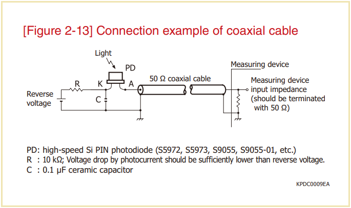
    such a circuit with a load resistor as shown below might make sense for "event detection" in a physical experminent or for optical communications, but not at all for precise light level measurements, especially not in low light level applications. You will suffer from all the disadvantages a good TIA is avoiding.

    Kai