Part Number: OPA694
Dear all,
I am Andrea Celentano, staff scientist at the "Istituto Nazionale di Fisica Nucleare" (INFN), working in the field of high-energy physics.
We are using the OPA694 to design a fast amplifier for a particle physics detector. In the past, we used this component in other circuits, with very good results.
I have a question concerning a detail of the PCB design, specifically the routing of the different signal traces for the OPA 694.
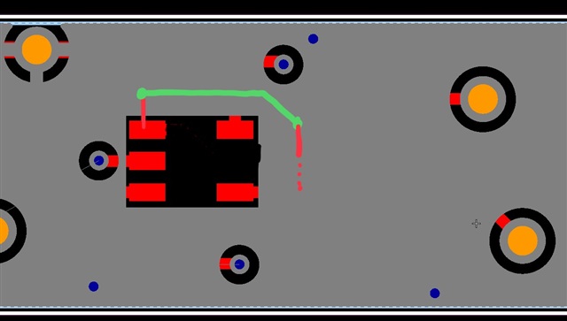
In the picture below, you find a view of the PCB we are designing. This is a 4-layers circuit.
The gray plane is GND. The traces in RED are on the TOP plane. The 6 pads are those were the OPA694 will be mounted (we use the SOT23-5 six-pins DRB package). The top-left pin is pin #1, output.
As you see, the GND plane is cut all around the OPA 694. However, we have a trace routed on the TOP layer, just below the OPA694 (for design reasons, there is no way to route this trace on the TOP layer in a different way).
An alternative would be to route this trace in an internal layer, by adding two vias, as I report in the image below, where the green trace is in a middle layer. In this alternative approach, the output signal trace does not run below the OPA694, but there are two vias in addiction.
May I ask you what is the preferred configuration, or if these are basically equivalent?
Thanks,
Andrea