This thread has been locked.

If you have a related question, please click the "Ask a related question" button in the top right corner. The newly created question will be automatically linked to this question.

OPA858DSGEVM: OPA858DSGEVM || TIA Design for 500MHz input frequency

Part Number: OPA858DSGEVM
Other Parts Discussed in Thread: OPA858, OPA855, TINA-TI, LM324, OPA859

Hi,

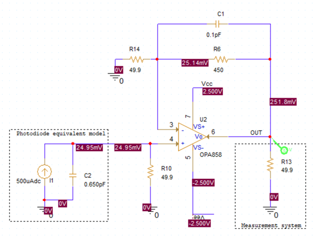
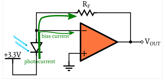
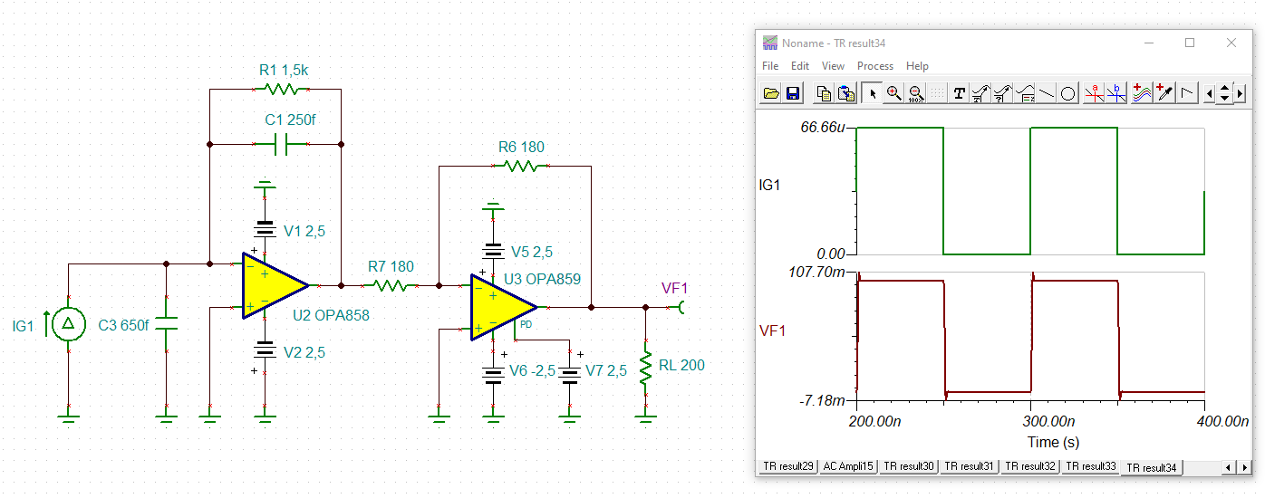
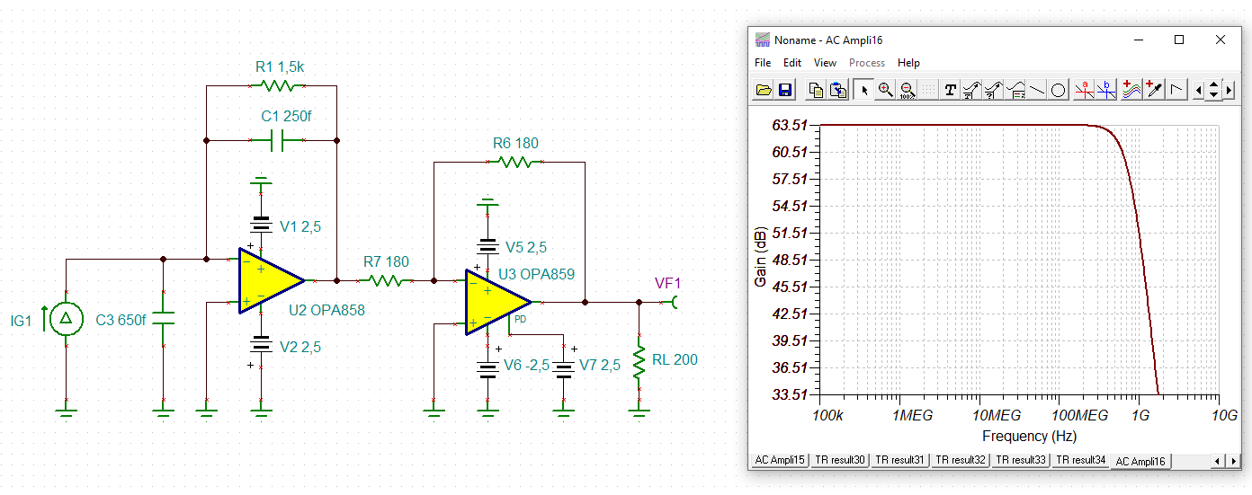
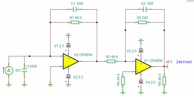
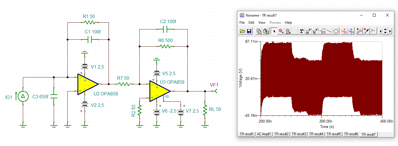
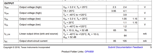
I purchased an OPA858DSGEVM from TI recently. I would like to design a stable transimpedance amplifier using this evaluation board. Please find below the photodetector specifications:

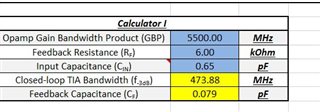
1)capacitance: 650fF

2)maximum current = 330uA

3)Maximum output voltage = 500mV

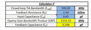
4)Bandwidth required = 500MHz

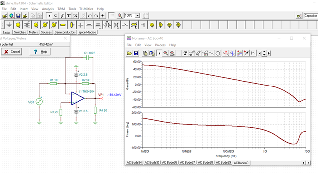
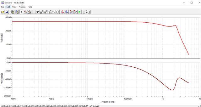
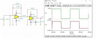
Could you help designing a stable TIA, please? The one I designed seems to oscillate.

  • Hi Kai, 

    Thank you for providing the links, Kai!

    Hello Shine,

      I would also suggest using this TIA calculator: e2e.ti.com/.../faq-transimpedance-amplifier-calculator

      From your provided specifications, you would need at an amplifier with at least 1.5GHz bandwidth with a feedback compensation capacitance of 0.3pF. With a higher bandwidth such as the OPA858, you may slightly increase capacitance to decrease the bandwidth. 

      This thread has simulation files that Kai has done that would be useful to determining stability of the OPA858 as a transimpedance amplifier. Kai has also provided a simulation circuit with varying feedback capacitance which I have included below as reference.

      This thread is useful if you are using the OPA858 EVM for TIA application evaluation.

    2086.raymond_opa858_1.TSC

    Thank you,
    Sima 

  • Hi Sima,

    Thanks for the information. But using the TIA calculator, I'm unable to get the values you mentioned in the comment. Could you provide a snapshot of the values entered or the detailed calculation? Additionally, in the TIA calculator, I guess the Open loop GBP is 5500MHz for OPA858 and 8000MHz for OPA855.

  • Hi Shine,

    do you already have carried out a TINA-TI simulation?

    Kai

  • I haven’t carried out a simulation yet but I tried to use the TIA calculator shared by Sima. 

    Additionally, the closed-loop frequency (which I suppose is the actual bandwidth of the op-amp when in closed loop), is pretty low in the range of 400Mhz as per the datasheet of OPA858 and OPA855. Then do you think it's possible to make a TIA design which works with bandwidth of 500MHz as mentioned in my query? Please help here...

  • Hello Shine,

       Here are the values I used in the TIA calculator based on your above design requirements and parameters:

    Thank you,

    Sima 

  • Thanks for the information but could you tell me why " datasheet range of 400Mhz as per the datasheet of OPA858 and OPA855." Does it mean the closed loop bandwidth is limited to this frequency?

  • Hello Shine,

      That is a good figure to point out. With higher feedback resistors, there will be a decrease in bandwidth. But since you only need 1.5kOhms, you should be able to hit 500MHz of closed loop bandwidth.

      Using OPA858 GBP at 6kOhms:

    It will be hard to realize 0.079pF, so increasing feedback capacitor to 0.1pF will bring closed loop BW to around 400MHz.

    Thank you,

    Sima 

  • Hi Sima,

    Thanks for the input. Now that we have decided to reduce the transimpedance gain factor to 500 with closed-loop bandwidth of 500MHz but we require a non-inverting output. The photodiode current needs to be measured from 0uA to 500uA and should give 0V and +250mV respectively.at the final output. Also, note that we cannot change the orientation of the photodiode because it's already embedded in a photonic chip and its anode needs to be connected to the op-amp input.

    But the issue I'm facing while using OPA858 is in the transimpedance configuration, during simulation is that I get an inverting output. This is because the photodiode cathode is connected to a positive bias voltage of +2V and and the anode as I mentioned is connected to the inverting terminal of the op-amp. Now, the solution I can think of is using another unity gain inverting op-amp configuration at the output of the existing transimpedance amplifier but wouldn't it add additional signal integrity issues and can I still get 500MHz bandwidth? Or is it fine if I take care of the PCB layout design well to achieve this bandwidth? I thought of using non-inverting configuration but wouldn't that take out the real essence of a transimpedance amplifier as we are simply using a termination resistor (say 49.9E) to convert current to voltage and then amplify the voltage? Would it have the same performance in all aspects as the inverting transimpedance amplifier? So my query is alternatively, whether we have a single op-amp solution to achieve a 0 to +250mV output with the given specifications by using some additional biasing techniques.

  • Hi Shine,

    you cannot replace a TIA by a non-inverting amplifier. These are totally different topologies. With the non-inverting amplifier you get an unwanted input voltage divider caused by the detector capacitance, stray capacitance and the input capacitance of OPAmp. Also, the photodiode current now causes an unwanted voltage drop across the input resistance R10 and by this changes the bias voltage of photodiode. You don't have any longer a zero bias voltage at the photodiode but a bias voltage which depends on the photodiode current. This means a change of sensitiviy of photodiode depending on the photodiode current.

    All the advantages of the TIA are lost...

    Kai

  • But the above configuration provides the same gain as an inverting configuration. 49.9x(1+450/49.9) = 499.9. Shouldn't it work the same way as well? If it doesn't, may I know the solution you suggest?

  • Hi Shine,

    you could do the inversion of signal this way:

    shine_ths4304.TSC

    Is your photodetector directly connected to the OPA858? What is the distance?

    Kai

  • Thanks. This seems good but could you tell me how this voltage got inverted in this setup? Also, would this mean I can get a positive dc swing from 0V to 250mV for 0uA to 500uA current if I set the gain correctly? Could you setup the gain for 500E see if the performance is still good?

    The photodetector used has a bandwidth of 2.5GHz but we need only 500MHz of bandwidth. This is still in design phase, so I could add the resistor in between the photodetector and the inverting terminal to obtain the right output. Here's a simple example to show just the photodiode biasing orientation;

  • Hi Shine,

    here's another inverter:

    shine_opa859.TSC

    To your question:

    The detector current direction through RF is correct. You would get a negative output voltage swing when the detector is receiving light.

    But the input bias current of OPAmp and the bias current through the photodetector (dark current) will flow through RF.

    May I ask again: Is your photodetector directly connected to the OPA858 or remote? What is the distance?

    Kai

  • Thanks. But there seems to be some confusion. Here's the analysis I got for the circuit you provided. When the gain is increased to 500E, the bandwidth is significantly degraded. Also, I want the output to be positive and not negative. This looks like it's giving a negative output. Am I missing something here?

    The photodiode is directly connected to the opamp as we require the DC variation with the laser variation. The photodetector is closely coupled to the laser light. Also, if you mean the PCB distance, we haven't done the PCB yet but we plan to place it as close as possible to the opamp input. 

  • Hi Shine,

    the idea is to mount the inverter behind the TIA to change a negative output voltage swing into a positive according to what you wrote here:

    But the issue I'm facing while using OPA858 is in the transimpedance configuration, during simulation is that I get an inverting output. This is because the photodiode cathode is connected to a positive bias voltage of +2V and and the anode as I mentioned is connected to the inverting terminal of the op-amp. Now, the solution I can think of is using another unity gain inverting op-amp configuration at the output of the existing transimpedance amplifier but wouldn't it add additional signal integrity issues and can I still get 500MHz bandwidth?

    Kai

  • Hi Kai,

    Now I get it but if this inverter is behind the TIA, you mean the photodetector needs to be connected to this setup? Could you show me the entire setup (the two stages) please? Also, why can't we have an inverter after the TIA to do the inversion? Could you provide details of that as well?

  • Shine,

    why making things so complicated? I said that the inverter should be mounted behind the TIA:

    shine_opa858.TSC

    Kai

  • Thanks. Now it's more clear for me. I have the following queries regarding the design;

    1) I have seen in some thread regarding OPA858 that the gain needs to be at least greater than 7V/V to be more stable. Is that the case? Also, to maintain just one line item in the BOM, can I use the same OPA858 IC for the inverter with a small gain? Something as shown below; Do you see any possible design issues with this at a circuit level or PCB level? I have attached the file belowtwo stage_opa858_1.TSC

    Gain = 49.9(stage 1) x (500/49.9) (stage 2) = 500 

    Bandwidth:

    2)What are the PCB design constraints that we need to take special care of to achieve a very stable version of this design?

    3) In the evaluation board of OPA858, I have noticed the extensive use of 49.9E resistors. Why isn't 50E being used instead? Is there a logical reasoning behind it?

  • Hi Shine,

    don't feel offended, but your questions sound very strange. Do you realize that we are not taking about a cheap 1MHz OPAmp like the LM324 but a decompensated 5.5GHz OPAmp here??

    Why not performing a phase stability analysis before posting such a mad circuit?

    Also, to maintain just one line item in the BOM, can I use the same OPA858 IC for the inverter with a small gain

    Is this your only concern? To get a short BOM list?

    Shine, you really should have some experience when doing in 500MHz circuits. You really should have some thorough understanding and at least know about the basics. But me thinks that you are only guessing...

    Kai

  • Hi Kai,

    Thanks for your inputs and patience in dealing with my questions. I'm new to this 500MHz based analog circuits even though I have done some high-speed interface design. Could you tell me why we are using 180E and 180E exactly and why not some other resistor values such as 50E and 50E to get unity gain? Also, I believe I can change the 1.5K to 500E to obtain the 500 gain and what would be Cf in that case? I just wanted to make sure I don't make any  mistakes in my design.

    2)What are the PCB design constraints that we need to take special care of to achieve a very stable version of this design?

    3) In the evaluation board of OPA858, I have noticed the extensive use of 49.9E resistors. Why isn't 50E being used instead? Is there a logical reasoning behind it?

    Also, the above questions, please.

  • Hi SHine,

    I just wanted to make sure I don't make any  mistakes in my design.

    There are so many mistakes that even don't know where to start. Do you know how an OPAmp works?

    Do you know that the load at the output of an OPAmp must not become too small? Because of this RL must not be 50R, R7 must not be 50R and R1 must not be 50R. All these resistors are too small and you short-circuit the output of OPAmp. Not only RL is a load to the OPAmp output but also R1 and R7 because they also force a current to flow from and into the output of OPAmp. Go into the datasheet to see what load is recommended and what feedback resistance is recommended.

    Don't make changes on a circuit, if you don't know the consequences. You cannot change R1 to any desired level in a TIA and you cannot change C1 to any desired level in a TIA. The detector capacitance, R1 and C1 must fit together. The phase stability analysis says what values fit together and what values do not fit together. Search in the forum for "phase stability analysis" to see how a phase stability analysis is carried out. The so called "phase margin" plays a key role in order to find a stable circuit. Also watch this TI's training video series on stability:

    https://training.ti.com/node/1138805

    The same is true for an inverting amplifier. You cannot change R6 and R7 to any desired level, because these resistors determine the load resistance for the OPAmps and have a deep impact on the frequency response and stability. Again, a phase stability analysis has to be carried out to find a good compromise between bandwidth and stability. This is especially true when you add C2.

    In the evaluation board of OPA858, I have noticed the extensive use of 49.9E resistors. Why isn't 50E being used instead? Is there a logical reasoning behind it?

    The reason for using 49R9 instead of 50R is very simple: You cannot buy a 50R resistor, usually:

    https://en.wikipedia.org/wiki/E_series_of_preferred_numbers

    Kai

  • Firstly, with all due respect, I was just asking a few questions which I felt were required for my design.

    Secondly, I completely understand the mistake of the circuit I posted and I'm only talking about the circuit you had suggested. Can I have 500 gain factor(in the design you mentioned, it's around 1.5K) and what would be the CF value? Here's a snap from datasheet which shows that we could go upto 10ohms of load. Also, in this case the maximum voltage is 250mV which means the maximum output source or sink current would be 250mV/50 = +/-5mA. I'm asking this because my load impedance at the other measurement end is 50ohms. Could you kindly suggest if I can still go with the circuit you recommended with a 50ohms load (as my measurement system is 50ohms load)?

  • Hello Shine,

      You may use a 500Ohm gain factor instead of the 1.5k. Using the TIA calculate above, the resulting Cf is at least 250f which will give you above 1GHz BW without accounting for additional parasitic on the board. 

      Using Kai's simulations: 


         Note: I did not run a full stability analysis, and would recommend following the simulation and threads that Kai and I posted in the first two replies. 

        With low voltages at the output of the second stage, that calculation is correct and it would be safe to use 50Ohm as the load. With higher output voltages, you would run into a loading issue. 

       However, you probably won't need a very high BW amplifier with the lower gain change:

       A two stage OPA859 design would work just fine. If you want the extra bandwidth/gain reserve, you may stay with the OPA858, but would have to be extra cautious with the layout compared to the OPA859. Still, both are GHz parts, and would recommend following the EVM for each device and the recommended layout section in the devices' datasheets. 

    Thank you,

    Sima