Because of the Thanksgiving holiday in the U.S., TI E2E™ design support forum responses may be delayed from November 25 through December 2. Thank you for your patience.

This thread has been locked.

If you have a related question, please click the "Ask a related question" button in the top right corner. The newly created question will be automatically linked to this question.

THS3001: Correct configuration for DAC output

Part Number: THS3001
Other Parts Discussed in Thread: OPA695, LMH6702, THS3217, THS3215, OPA684, THS3092, OPA4872

Dear all,

I guess it is a simple question but due to my lack of experience in analog electronics I would like to be sure of what I do.

I am using AD9707 DAC from Analog Devices. I want to single-ended buffer the output as in pag. 40/42 of the datasheet but using THS3001 instead of ADA4899. I have configured the DAC so IFS=2mA (RSET=16K)

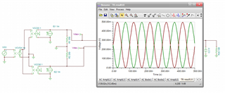
I want VOUT (after the THS3001) to be 2Vpp (-1V/+1V).  I trying to use similar schematic as in DAC datasheet and I have simulated with TINA but without success. Please find attached an image of the simulation.

DAC is simulated as a current source 0-2mA. For Rs I am  using 49,9Ohms. REFIO is 1V (Internal of DAC)

How should be the schematic for the output I need? Is the DAC well simulated with a current source of 0-2mA? If not, how should I simulate it? is RS correct or what other value should I use?

Thanks in advance.

Joaquin

.

  • Well Joaquin, number of issues here, 

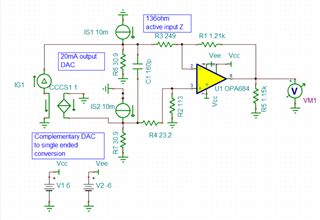
    1. These comms DAC's are always complementary current output - they are steering a tail current (2mA) between two ouptuts - so you need to model that. 

    2. Normally, you want to use both output currents to get the best HD2 suppression and convert to single ended in the amplifier stage 

    3. The THS3001 is NRND, it has some performance hazards - on +/-5V you should probably look at the OPA695 or LMH6702 wideband CFA

    4. Or, even better, use the THS3215 or THS3217 that are specifically intended for this requirement, 

    Here is an example design using the much slower OPA684, this is for a 20mA peak output so it has 10mA DC on each side and inverterd +/-10mA full scale current sources to emulate the DAC, this gets real complicated if you try to match load Z on each side as this design shows an active input Z on the inverting side. The THS317 bypasses all of those issues. 

    Complementary to single with OPA684.TSC

  • Hi Michael,

    Thank you for your repply and sorry for my late answer.

    After study your email, I have decided to go for THS3217 as a mean to get a single output from de DAC.

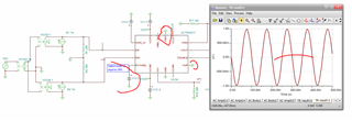
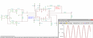
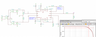
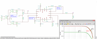
    Please find attached an image of the simulation with TINA for my system. I have simulated the DAC output as you did in your example but for 0-2mA.

    The schematic is derived from the schematic in the first page of THS3217 datasheet. As this schematic gives an output of VO=5xVI, I have added two resistors of 100R at the input so the current input is converted to voltage.

    Do you see any problem in this schematic? Is correct to place two resistors of 100 Ohms at the input?

    I am not able to see clearly on the THS3217 datasheet the gain formula. Can you explain me how to configure other gain in the THS3217? I see that the gain on hte D2S stage is 2 and the gain for the OPS is 2.84, so the gain should be 2x2.84= 5.62 not 5.  What is wrong?

    Thanks in advance,

    Joaquin.

  • Hi again Michael,

    Forget about the Gain, I have already seen it. Sorry for the confusion.

    The other questions are still on, I would appreciate any comment on the input resistenace.

    Regards,

    Joaquin.

  • Well were I would start is on what the DAC can safely produce at its output. 

    With the OTCM pin at ground (apparently a way to offset the output CM voltage) and +/-2mA coming out of each pin, the DAC says it can handle a compliance voltage range of +/-0.8V. So, let get it to produce a 0 to 0.5V on each output line using a 250ohm termination R. Often, A filter is included here to roll off the image frequencies. but not for now, this is another way to set up the source currents I had in an old THS3217 file, I am just looking at the voltages at the THS3217 inputs here at 10Mhz (not sure what your speed is, if it is not too high, consider the lower power THS3215 as a functional equivalent). 

    From this, you said you wanted a +/-1V output. Ok, I think the D2S stage can do this by itself and you can just disable the output power stage. Not sure about your load, but perhaps a series 50ohm to a termination 50ohm - is the +/-1V at the termination maybe? Ok, so the D2S will put out a ground centered +/-1V from this input, I have simply grounded the Vref pin where you don't need to use the internal buffer feature unless you want to move this common mode around at the D2S output. 

    The OPS is not disabled, but not used here - yet, I just grounded its V+ input for now, 

    So lets say you really want +/-2V at an OPS output to drive into a 50ohm cable and take a -6dB insertion loss, Let's run the D2S into that V+ input on the OPS externally as it is now (often this is another place to add a RLC filter) and set the OPS up for a gain of 2- it is just a CFA amp, so raise the Rf value a bit to run gain of 2, Here that is looking quite nice at the matched load, Again - the THS3215 operates the same way, just a little slower with less quiescent power. 

    And lets do a small signal AC sweep, probably peaking a little - maybe a good reason to add a filter into the OPS V+ input, noo pretty bandlimited at 138MHz, maybe that 250ohm at the inputs are bandlimiting with the input C term to the buffers - does this look good enough? yea, 2.4pF and 250ohm is about 265MHz, maybe the D2s is slowing that down some - essentially, I was expecting this to be more like 600MHz BW.

    Here is this file, 

    AD9707 output to THS3217.TSC

  • yes, I think the bandlimiting is at the inputs due to the 250ohm R's and the C. Including the diff C of 2.8pF, this should bandlimit below 100MHz. Is that ok? if not, the R's will need to be reduced and more gain moved into the OPS stage. 

    here is the response shape at each node, 

  • Hello Michael,

    Thank you very much for your support. Sorry for my late answer but other project have keep me bussy.

    The only thing that I dont understand from your emails is the place for C=2.8pF. Are you talking about to add a C 2.8pF in the inputs? From input to input? or From inputs to GND? or what you mean when talking about C?

    Our bandlimit is about 40Mhz-50Mhz , so 250 Rs are OK and I will probably go for the THS3215 as you suggest.

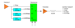
    Althought the next question has not to do with our previous discussion, please let me do a new question. After the THS3217 our customer want to select between  +-10Vpp, +-1Vpp, +-0.1Vpp and +-0.01Vpp. So What I am think is to, for example configure THS3217 to have an output +-5Vpp and then, use voltage dividers to get +-0.5, +-0.05 and +-0.005 V. Then use a multiplexor (for example TMUX6104PWR) to select the output and after the multiplexor, place a non  inverter amplifier as THS3092 with G=2.

    Please find attached a blok diagram which I expect you are able to understand me.

    With this configuration it would be possible to chose between +-10Vpp, +-1Vpp, +-0.1Vpp and +-0.01Vpp.

    Do you see any problem in this? Do you see a better way to do this?

    Thanks again for your support.

    Regards,

    Joaquin.

  • Morning Joaquin, 

    The 2.8pF is inside the THS3215 or THS3217, 

    Yes, ranging with attenuators is one way, you just have to be careful that stage can handle these higher slew rates. Mux's have their own issues, we have in the past done this with buffered Video mux's like the OPA4872 - look at Figure 29

    https://www.ti.com/lit/ds/symlink/opa4872.pdf

  • Hello Michael,

    Thank you very much for your quick answer.

    I will considerer OPA4872.

    Regards and happy weekend.

    Joaquin.