- Ask a related questionWhat is a related question?A related question is a question created from another question. When the related question is created, it will be automatically linked to the original question.
This thread has been locked.
If you have a related question, please click the "Ask a related question" button in the top right corner. The newly created question will be automatically linked to this question.
Hi Team,
Good day! Could you help us with our customer?
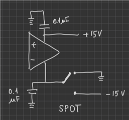
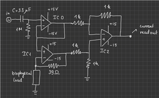
Certainly, I have a little circuit that I built to keep a constant AC voltage across some biophysical sample (attached) that can also measure the current through the sample. I am currently using op amp TL071IP, which works fine for the most part. The issue is the current that feeds the load comes from the op amp, which is fine, but the TL071IP can only source or sink around 10mA (if I read the datasheet correctly). I am looking for an op amp with similar characteristics, but can source or sink, let's say >50mA. I recently bought TLC071AIP. This one can take single or dual supply. So I connect Vdd to 15V and ground to zero for single supply. But it didn't work as I expected. I am wondering if there is anything wrong with the way I use this op amp.
that would be nice. Another question is: when I connect a function generator to the input, there are some spikes when I vary the frequency, and this creates disturbance that impacts my sample. So I put a high pass filter to the input. And it seems that this stabilizes it
but how should I reconcile this with the fact that spikes are like high frequency signal
and this high pass should pass it through instead of blocking it
basically I'm just wondering if a high pass filter is a reasonable thing to couple to the input in this situation
That will be it. If TLC071AIP doesn't work, please recommend me something that work. I will be looking forward to your answer. Thank you so much!
Best regards,
Jonathan
Hi Jonathan,
I think we are talking about IC1? Well, when your input signal voltage from the function generator is going negative the input voltage of single supplied IC1 leaves the allowed input voltage range of IC1 which is > +0.5V. And as you even go outside the supply voltage of TLC071 you risk a damage of IC1. So when your biological load shall be driven by an AC signal, IC1 should not be powered by a single supply.
Can you tell more about your biological load? Is it resistive? Is there a cable connected? Does it generate an EMF (voltage)?
Kai
Hey Jonathan,
Quick note here, the TLC071 has a higher output current but the max supply voltage is lower, and will not work at +/-15V. Have you considered the OPAx990 family of devices? It's a much newer device, with 80mA of output current and can be supplied from +/-15V supplies.
Best,
Jerry
Hi Kai and Jerry, thanks for letting me know that I shouldn't use single supply for AC signal. It seems all the IC's need to be dual supply although it is IC1 that drives the load right?
The load works more or less like a continuous RC transmission line, although its departure from that is what we are interested in. It consists of a buffer saline solution sandwiched between a resistive Cr and Au layer and another Cr & Au layer (coated on glass slides) which serves as ground electrode. This altogether is sealed in a chamber with epoxy. The ions in the solution act as a distributed capacitor through the forming of electric double layer next to the resistive metal layer. We can vary the resistance of this layer.
The inverting input of IC1 is connected through a BNC cable to this load. I don't think it generates EMF.
Another problem is the current readout is quite noisy. It is much noisy if I use a DIN rail +/- 15V power supply, and less if I use +/- 16.9V batteries. I already put decoupling capacitors in. I am wondering what op amp I should use, or how to modify the circuit to reduce the noise in the combination of the current to voltage converter (IC1) and differential voltage amplifier (IC2). Does this have anything to do with bias input current I_bias and offset current I_offset?
Hi Jerry,
Thanks for the suggestion. I will take a look. But does this family have DIP-8 package? It would be better like that because I solder my circuit to veroboard in my lab. Can you send me the link to this family? I guess my application needs something low noise, so I am wondering if there is any characteristics we trade for the 80mA output of this family?
-Tri
Hi Tri,
It seems all the IC's need to be dual supply although it is IC1 that drives the load right?
Yes, if you want to proceed with this circuit.
The load works more or less like a continuous RC transmission line
Can you specify the total capacitance of this transmission line? I ask because a too high capacitive load at the -input of OPAmp will destabilize the OPAmp.
You could do it this way:
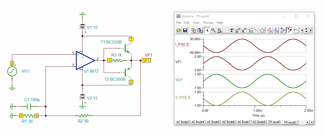
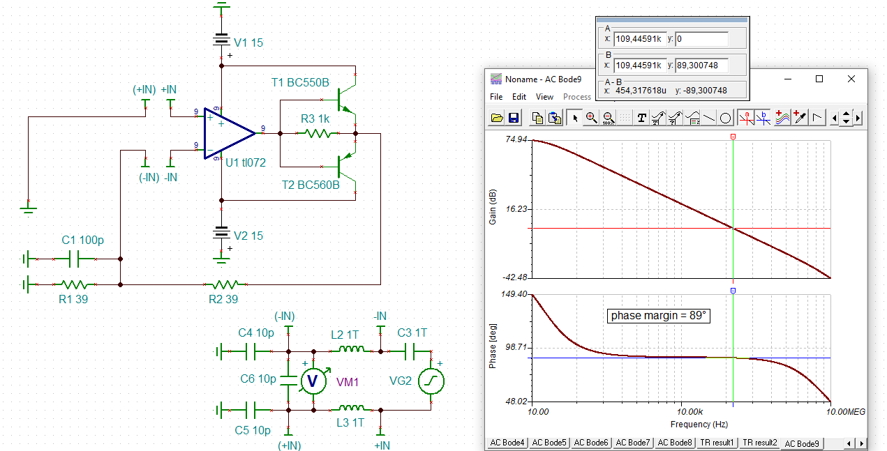
C1 represents the unavoidable capacitance of transmission line. So don't add C1.
Another problem is the current readout is quite noisy. It is much noisy if I use a DIN rail +/- 15V power supply, and less if I use +/- 16.9V batteries. I already put decoupling capacitors in. I am wondering what op amp I should use, or how to modify the circuit to reduce the noise in the combination of the current to voltage converter (IC1) and differential voltage amplifier (IC2). Does this have anything to do with bias input current I_bias and offset current I_offset
Instability could be the cause of noise. A low pass filter could be added at the input of IC0. The supply voltage should come from a proper voltage regulator like the LM7815/LM7915, e.g. The four 1k resistors should be increased to 2k...10k. Add identical NP0 filter caps at the differential amplifier from the +input to ground and from the -input to the output. Take 33p...100p for a start. Add a 100R isolation resistor at the output of last OPAmp.
The noise can also come from the chemical process itself, if there's any dynamics in the fluid.
And finally, IC1 itself can become instable when the resistance of the biophysical sample becomes too high. In this case mount a resistor in the 100R to 1k range in parallel to the biophysical sample (R1 in my circuit) to guarantee a minimum gain preventing a loss of phase margin. Play a bit with my simulation. If the resistance of the biophysical sample becomes too low ohmic, on the other hand, the gain of IC1 can become huge and this can result in a highly amplifying of OPAmp noise, biophysical sample noise or noise coming from the function generator.
To optimize the circuit you should find out the capacitance of transmission line and the resistance range of biophysical sample. For best performance the resistance range should be limited somehow. It should neither be too small nor too big.
Kai
Nice, it will take me sometime to understand all what you recommended. Quite a few things are new to me. I understand that
jonathan_tl071.TSC
this has a push-pull buffer. This can provide both the signal to the sample as well as measured the current, which is now provided by both the op amp and the power supply.
The total capacitance of the sample, by the way, is around 25μF.
The rms voltage I put across this sample is less than 1 V (usually 100-500 mV) as we don't want electrolysis to happen in the chamber.
I will study what you recommend for reducing noise further.
How do I open the tsc by the way? Is that a tool to create and virtually test electronic circuit?
Hey Tri,
You can open a .tsc using TINA-TI
Here is the link to download it: https://www.ti.com/tool/TINA-TI
Best,
Jerry
Hi Kai and Jerry,
@Jerry, thanks for pointing me to TINA. I think I start to get a grip on how to use the software.
@Kai: let me clarify what I said with some TSC files. I'm wondering if I should add some resistors to make sure the output wattage is not too strong. Earlier, I made a pushpull buffer as in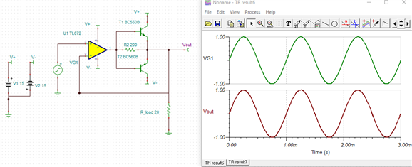
It burned my sample as I connected this pushpull to it. I suspect that was because of the +/- 15V power supply connected directly to the sample through the transistors.
To limit the current to some maximum value, I added some resistances like this.
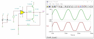
Following your suggestion, I also rearranged it to convert current to voltage as well.
My question is would adding resistors R1 and R3 like I did help limit the current as I wanted? The output voltage from Tri_push_pull_2 isn't a sine wave. Is that because that is the sum or difference of 2 sine waves?
Also, can you explain what is the circuit bounded by the (+/-IN) and +/-IN jumpers? What is the function of that?
I incorporated what I understand of your recommendations in the following circuit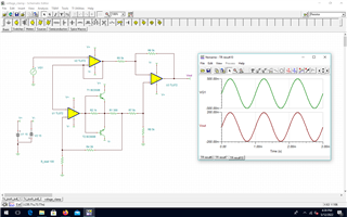
voltage_clamp.TSC
Could you take a look and edit directly on this file what you think would be best?
Thanks,
Tri
Hi Tri,
hmm, I fear that 25µF is too much for this circuit. This is just too much capacitance from the -input of OPAmp to ground.
Kai
Hi Tri,
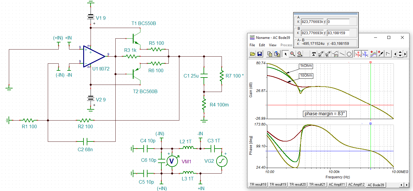
I would do it quite old school and put the biophysical sample in series with a 0.1R shunt resistor and amplify the voltage drop across this shunt resistor. This will ease the situation a lot:
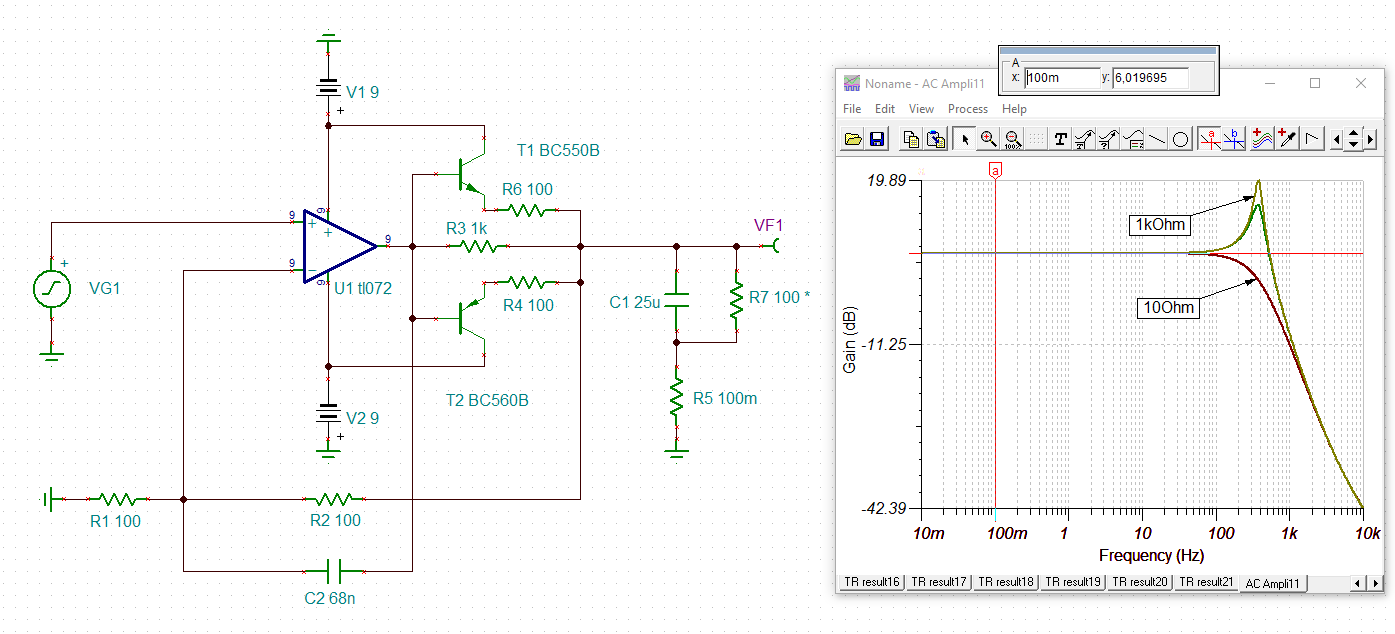
You will notice that due to the extreme capacitance of your biophysical sample the bandwidth cannot be very high.
To ease the current limiting of this circuit the supply voltage was reduced to +/-9V.
If the offset voltage shall be minimized, a big capacitance can be put in series to R1. Also, the offset adjusting scheme of the TL071 could be used. Of course, an OPAmp with lower input offset voltage could also be used. But in this case the phase lead compensation would have to be comfirmed.
The phase margin is quite good:
Kai
Hi Kai,
I have a few questions regarding your design and suggestion. As a physics major, I am still learning a lot about electronics, so I really appreciate if you could help me clarify these points.
1. What is the function of the lower left part of the design (with question mark)? I don't see how the voltage put across the load is the same as the AC source.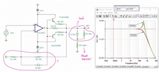
2.
To ease the current limiting of this circuit the supply voltage was reduced to +/-9V.
suppose I want to keep using the +/-15V supply, can I increase R4 and R6 to say 200 Ohms?
3.
You will notice that due to the extreme capacitance of your biophysical sample the bandwidth cannot be very high.
In my application, I actually want to probe frequency up to 100 kHz. Is there any way I can improve the bandwidth? Is the limitation in the quote the same regardless of OP AMP and BP transistors? Or we can choose other op amp and transistors?
I actually built a variant of the push-pull buffer with TL071IP, and MJE2955T and MJE3055T as follows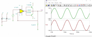
The output at first was a clean sine wave, but it was not quite stable and got distorted when I tried connecting it to different loads. I am not sure why that happened.
I took some data with this version, and it seemed I could go to up 50 kHz with some biophysical load of the type I described.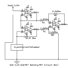
4. I don't understand what you mean by this.
If the offset voltage shall be minimized, a big capacitance can be put in series to R1
and this
Also, the offset adjusting scheme of the TL071 could be used.
5. Now that I think about this starting design in my project
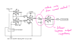
Is the function of the low pass filter in this circuit to filter out the noise in the current measurement? Suppose, I have signal at 50 kHz, will it work if I design the low pass filter to have cutoff frequency at 100 kHz?
6.
amplify the voltage drop across this shunt resistor.
Could I implement this with this non-inverting amplifier or something different?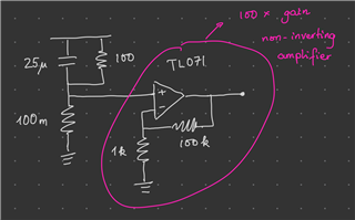
I know this is a lot to ask, but if you think we'd better discuss this on zoom, that would be great too.
Thank you in advance,
Tri
Hi Tri,
1. What is the function of the lower left part of the design (with question mark)? I don't see how the voltage put across the load is the same as the AC source.
The OPAmp runs at a gain or 2V/V here. This has stability reasons because a unity gain follower with a gain of 1V/V is way less stable. R1 and R2 set the gain and because this is a non-inverting amplifer and R1=R2 the gain is set to 2V/V.
It has turned-out that bigger values for R1 and R2 than 100R are disadvantageous and result in a lower bandwidth of circuit.
C2 is a very important component. It's the phase lead capacitance restoring the phase margin and making the circuit run stably. You cannot run this circuit without this very important phase lead capacitance.
R3 and the transistors isolate the output of OPAmp inside the feedback loop from the capacitive load and introduce a phase lag. C2, on the other hand, connects the -input of OPAmp directly to the output of OPAmp and by this introduces a compensating phase lead. The scheme looks like the so called dual feedback method which is discussed in this TI's training video series on stability:
https://training.ti.com/node/1138805
The other questions I will answer later.
Kai
Hi Tri,
1. What is the function of the lower left part of the design (with question mark)? I don't see how the voltage put across the load is the same as the AC source.
C1 and R7 is your biophysical sample. I have assumed for R7 a range of 10R...1k. And yes, R5 is the shunt to measure the current. The idea is to keep the shunt sufficiently small, so that the signal voltage is almost totally dropping across the biophysical sample and only a fraction across the shunt.
suppose I want to keep using the +/-15V supply, can I increase R4 and R6 to say 200 Ohms?
The problem is that R4 and R6 must not become too big because this will increase the unwanted phase lag. And because you said that only about 500mV is applied to the biophysical sample, there's no need for an all too high supply voltage anyway.
You can try to increase R4 and R6 but must confirm that the phase margin is still ok.
In my application, I actually want to probe frequency up to 100 kHz. Is there any way I can improve the bandwidth? Is the limitation in the quote the same regardless of OP AMP and BP transistors? Or we can choose other op amp and transistors?
At 100kHz the impedance of 25µF is 0.064R. Applying 500mVrms will cause a current of 7.9Arms through the biophysical sample which seems to sound a bit unrealistic.
I actually built a variant of the push-pull buffer with TL071IP, and MJE2955T and MJE3055T as follows
The bigger the transistors in the buffer stage the higher the junction capacitances and the more difficult to provide the phase lead compensation. You can try to choose transistors allowing a bit more power, like the 1.5A transistors BD135/BD136. But replacing the BC550/BC560 by the 10A transistors MJE2955/MJE3055 seems highly unrealistic to me. You would need a buffer for the buffer then.
I took some data with this version, and it seemed I could go to up 50 kHz with some biophysical load of the type I described.
You said that the capacitance of biophysical sample is 25µF. So it isn't 25µF?
If the offset voltage shall be minimized, a big capacitance can be put in series to R1
The input offset voltage of TL071 will also be amplified by a factor of 2V/V. A cap in series to R1 will decrease the DC gain from 2V/V to 1V/V and by this the DC offset voltage dropping across the biophysical sample.
Also, the offset adjusting scheme of the TL071 could be used.
Datasheet of TL071 shows in figure 7-3 how to zero the input offset voltage. This was mentioned by me because DC voltages dropping across your biophysical sample might be unwanted.
Could I implement this with this non-inverting amplifier or something different?
Yes. You could even decrease the gain setting resistors by a factor of 10. And you can mount a cap in series with the lower gain setting resistor to keep the DC offset voltage low.
I know this is a lot to ask, but if you think we'd better discuss this on zoom, that would be great too.
The contributions here in this forum I do in my sparetime, for fun. I don't get any money for it. Starting a zoom discussion would be way beyond my possibilities
Kai
Hi Tri,
I think the crucial point here is that you should dramatically narrow the requirements of your circuit, if this is possible at all. Can you try to formulate an exact equivalent circuit model of your biophysical sample, in terms of capacitance and resistance? Are you sure that a transmission line is formed and that the capacitance of this transmission line is really 25µF? This would be a really huge transmission line. Are you really sure that it is 25µF? If the capacitance was way smaller, it would be way simpler to find a suited circuit.
And what current has to be driven. If it is only 50mA maximum, then no big transistors would need to be used. Yes, even a suited OPAmp could be used without any buffer stage.
Or can the application be divided into different requirements? That you can use a higher frequency circuit for a biophysical sample with a lower capacitance and - vice versa - a lower frequency circuit with a higher capacitance? And the same with the measurement current?
Kai
Hi Kai,
Thanks for taking time to reply me. You raised a good question, and I just ran some fitting to my data to determine the capacitance of the biophysical sample.
The samples look like this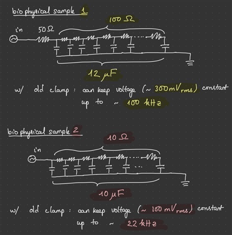
They consist of a distributed (continuous) resistive 2D layer in contact with an ionic solution, which we can model as a distributed (continuous) capacitance. The total capacitance is around 10-12 μF. Note that biophysical sample 1 has a trailing resistive layer of ~50 Ω. I have an analytical formula for the impedance of these model circuits.
I have a relative freedom in setting the value of the continuous resistive layer (can just adjust the thickness of metal deposited on glass slide).
I guess the sample isn't exactly like the resistance in parallel with the cap in your model. That might explain why with the voltage clamp I had earlier I could go up to 100 kHz for sample 1 and 22 kHz for sample 2?
I estimated that the maximum current for this application would be somewhere from 50-100 mA, as anything larger than that will burn the sample. As you said, we can do this with a suited OPAMP, and I'm also interested in learning about this push-pull buffer.
I chose the big transistors because I learned about the push-pull from the Art of Electronics book by Horowitz where they use these transistors for large currents. Since I was not sure how to choose transistors for my application, I decided just to go with them for a start.
Thanks,
Tri
Hi Tri,
yes, this considerably simplies the design. You could do it this way with your original circuit:
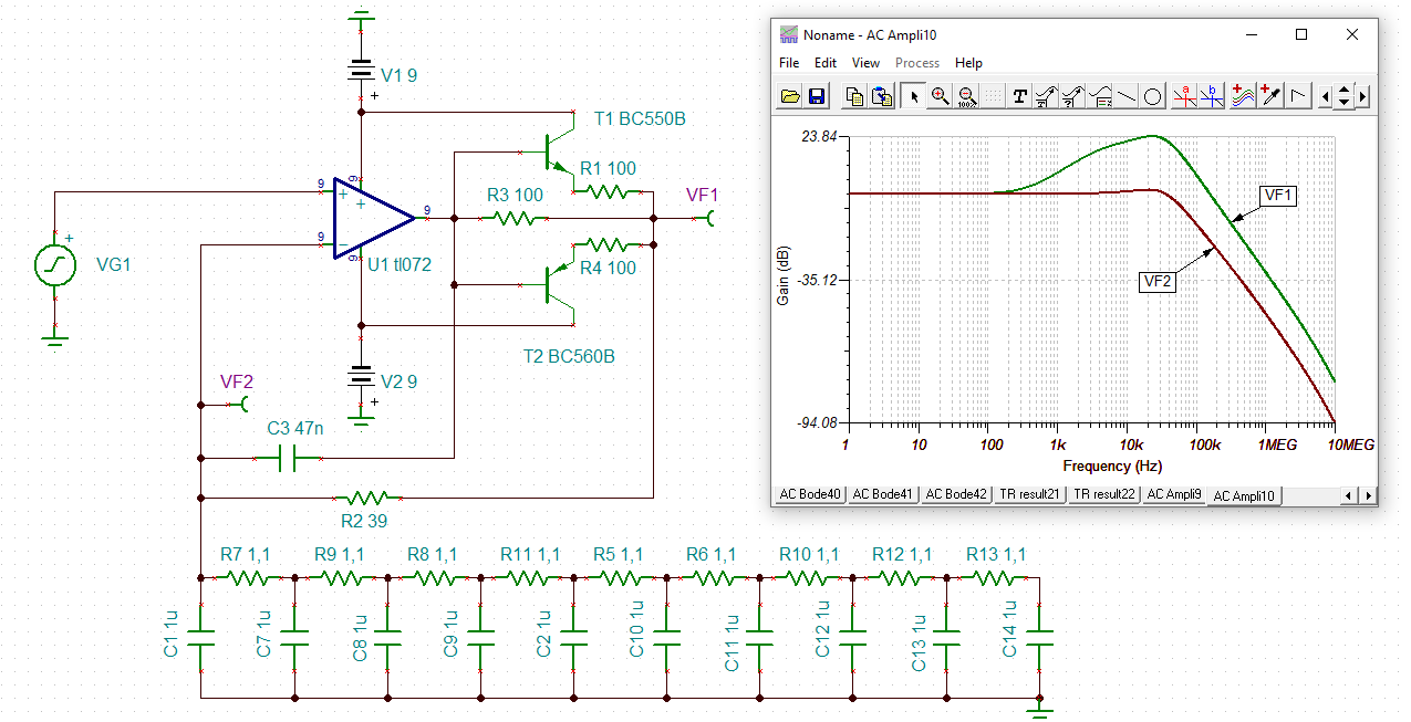
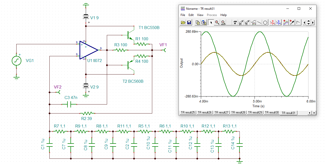
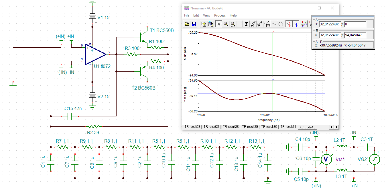
This isn't optimized yet. But at least you know now how to proceed and what techniques have to be used to make the circuit run.
You see that the gain of TL071 is considerably rising arround 10kHz. Because the TL071 hasn't much gain reserve at these frequencies, the distortion will increase noticeably. You might want to take a faster OPAmp and/or reduce the gain by decreasing R2?
In any case this is a very demanding application and you will need to spend some time and efforts to make the circuit run stably. The phase lead capacitance C15 is the key for stable performance and finding a proper value for C15 will be the central issue here.
Kai