This thread has been locked.

If you have a related question, please click the "Ask a related question" button in the top right corner. The newly created question will be automatically linked to this question.

THS3092: Harmonics Everywhere in the circuit

Part Number: THS3092
Other Parts Discussed in Thread: CDCE925

Hello

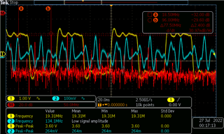
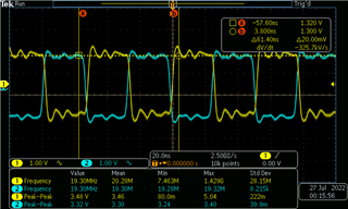
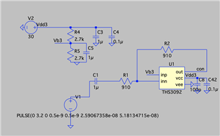
I am using CDCE925PWR to generate 19.3Meg Hertz Square wave. to feed into this THS3092. As soon as I turn on the opamp, I am seeing everywhere in the circuit that I have 260mV peak to peak in every DC input I have. I have 5Volts input from wall adapter to go into 3.3V LDO, and 1.8V LDO. I am seeing this(figure3) everywhere in the circuit. I ran fft and the frequency component of it was multiple of 19.3Meg hertz. I am able to operate Pll and generate this squarewave without this fluctuation, but just when I connect this to the THS3092 I am seeing this type of fluctuation. In figure 4, I am getting correct input and output wave. I am really confused why this might be happening. I have been stuck at this problem for weeks, and would you please help me out?

Thank you
  • Hi Young,

    I miss the isolation resistor or termination resistor at the output of THS3092. How do you connect the scope to the output of THS3092?

    Just to confirm: The supply voltage of THS3092 is +30V single supply?

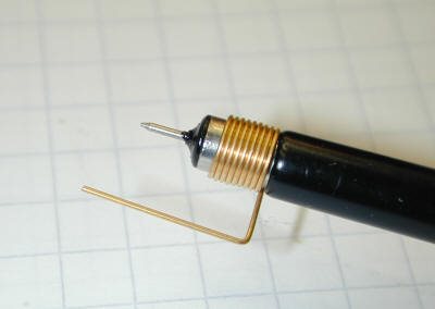
    Does your board habe a solid ground plane and are you following HF design practises? The ringing can come from an unsuited scope probe. Use such a scope probe with a ground spring:

    Kai

  • Yes. I have 4 layered PCB board, and I am using TPP 0250 probe having top capacitance 3.9 pF. Could that be a problems with the biasing the circuit?

  • Yes supply voltage is 30V single supply

  • Hello Young,

       How are you connecting the PLL to the THS3092? Would it be possible to input a square wave from a source generator at C1? I agree with Kai, it could be that you need an isolation resistor for the scope probe due to its capacitance. Figure 8 in the THS3092 datasheet recommends around 40-50 ohms series resistance prior to output scope measurement.

    Thank you,
    Sima

  • i am connecting the PLL output to the C1 Capacitor. I could see the frequency in the ground plane, and vdd and everywhere in the circuit. Could this be the ground bouncing issue? I don't see anything like this, but when I connect the THS3092, I am seeing this issue. and I am seeing like 30mv p2p 19.3 mhz wave everywhere in my circuit.. I am really confused

  • Hi Young,

    the CDCE925 is a very fast chip and generating a 20MHz square wave may make lots of noise. I think you will need Pi-filters at the supply voltage pins to prevent the harmonics from spreading over the whole board.

    Have you carefully followed the "layout guidelines" in section 12.1 of datasheet? Have you cut the ground plane under the crystal?

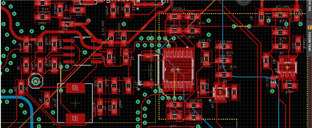
    Can you show some photos of your setup and the printed circuit boards? Can you show the layout(s)?

    Kai

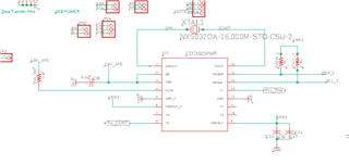
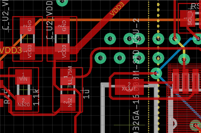
  • On the right is the PLL, and its supply voltages. There is a pin that is pretty close to Vdd like this one. Do you think this might cause the issue(below picture)? I am just using 30volts from power supply. I am not using DC/DC converter yet. 30 volts DC is from the power supply.

  • Hi Young,

    there are several issue:

    1. Decoupling caps must sit directly at the pins 3, 6 and 9. Your decoupling caps are way too far away. With this huge distance they appear to be not present. So your chip isn't properly decoupled.

    2. The signal ground must be connected to the pins 5 and 12. But I don't see any connection to signal ground.

    3. Also, the signal ground needs to be connected to the underlaying solid ground plane by many vias and these vias need to be placed close to the ground pins of CDCE925. But I don't see any vias.

    4. I also miss the many ground vias close at the ground terminals of decoupling caps.

    5. Use ground fills on the top and bottom layer and connect them with many vias (every 5mm or so) to the underlaying solid ground plane.

    6. Don't run the output signals directly without any isolation, termination or filter resistors over the board. These signals must be routed impedance controlled by using microstrip or stripline technique.

    7. The signal of pin 14 should not be routed in a loop arround the one terminal of crystal.

    You may want to have a look at this example layout which I made for another thread, to see how ground fills, ground vias, decoupling caps and the solid ground plane should be treated in a HF circuit:

    https://e2e.ti.com/support/amplifiers-group/amplifiers/f/amplifiers-forum/1086289/opa847-opa847-oscillation-for-embedded-gain-transimpedance-design

    See how close the decoupling caps are placed to the chip and how many ground vias are used to bond the ground fills and the ground terminals of decoupling caps to the solid ground plane.

    Kai 

  • The signal ground is connected to pins 5 and 12 they I am using toplayer as the ground plane. What is the output resistance required in the output of the PLL? My pll is working fine, but the issue rises only when I connect to the THS 3092. Do I have to redesign the PCB board to resolve this issue?

    Young

  • Hi Young,

    I am using toplayer as the ground plane.

    Is the top layer the components side? Using the component side as ground plane is no good idea. You cannot form a true ground plane with this method. You definitely need a separate plane only for signal ground. You urgently need a solid ground plane. "Solid" means "not interrupted", "without any gaps".

    What is the output resistance required in the output of the PLL?

    Datasheet of CDCE925 makes recommendations. See figure 5.

    My pll is working fine, but the issue rises only when I connect to the THS 3092.

    No, the PLL is not working fine and this has nothing to do with the THS3092. Please see the recommended layout in figure 24 in section 12.2 of datasheet of CDCE926. You haven't followed any of the recommendations given there. Haven't you noticed the boxes 1...4? Your layout looks totally different and is not well suited for the job.

    Do I have to redesign the PCB board to resolve this issue?

    Yes, I think so. And please follow the tipps given in figure 24 of datasheet of CDCE925.

    Kai

  • Hello Kai,

    I have 4 layered pcb. 1st,3rd, and 4th latyer is designated as ground plane. I am using 2nd layer as VDD plane where I have pads for vdd such as 30volts, 5volts, 3.3 volts. Do you mean that the first layer I shouldn't designate this layer as ground plane at all? Can I redesign the PCB and show you if that looks okay to you before I populate another PCB board?

    I really appreciate all the recommendation you gave.

    Thank you

    Young

  • Hi Kai,

    To add on my previous comment. How do you recommend routing the signal from PLL to the input of the THS3092? Do you recommend certain layer I should use? I really want to minimize the harmonics for my case..

  • Hi Young,

    Can I redesign the PCB and show you if that looks okay to you before I populate another PCB board?

    Yes, of course. I or someone from TI will surely have a look at your layout.

    I have 4 layered pcb. 1st,3rd, and 4th latyer is designated as ground plane. I am using 2nd layer as VDD plane where I have pads for vdd such as 30volts, 5volts, 3.3 volts.

    When the top layer contains the components you should use the second layer as solid ground plane. Otherwise the supply voltage noise will stray couple into the signal traces and components. This in combination with the wrong placement of all decoupling caps can be the cause of your huge noise problem.

    When using LRC-filtering at the supply voltage pins (Pi-filters !) a VDD plane for the CDCE925 may not be necessary. That's how I proceed in mixed analog digital circuits. I use pi-filters at the supply voltage pins of every analog and digital chip and don't use supply voltage planes. The free plane(s) I use for signal ground. Yes, I usually do have more than one solid ground plane.

    Do you mean that the first layer I shouldn't designate this layer as ground plane at all?

    The top layer with the components and signal tracks should be completely filled with signal ground to form so called "ground fills". The ground fills must be connected to the underlaying solid ground plane by as many vias as possible, at least every 5mm or so. The ground fills are extremely important in a HF circuit because they very effectively shield signals against each other.

    To add on my previous comment. How do you recommend routing the signal from PLL to the input of the THS3092? Do you recommend certain layer I should use?

    A certain layer is not necessary when you route the signal on the top layer and have a solid ground plane in the second layer. But in any case add the termination resistor of figure 5, mount it directly to the output of CDCE925 and try to route the signal to the THS3092 over a 50R microctrip line. The THS3092 should be placed close to the output of CDCE925 to keep the signal length as short as possible.

    Your layout arround the THS3092 should also be optimized. Look how the EVM in the datasheet of THS3902 places the feedback resistors. Don't use too long copper tracks here. Every millimeter counts.

    Kai