This thread has been locked.

If you have a related question, please click the "Ask a related question" button in the top right corner. The newly created question will be automatically linked to this question.

LMC6041: About Guard Ring

Guru 21045 points
Part Number: LMC6041

Hi Team,


I have four questions.


-------

[Q1]

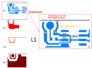
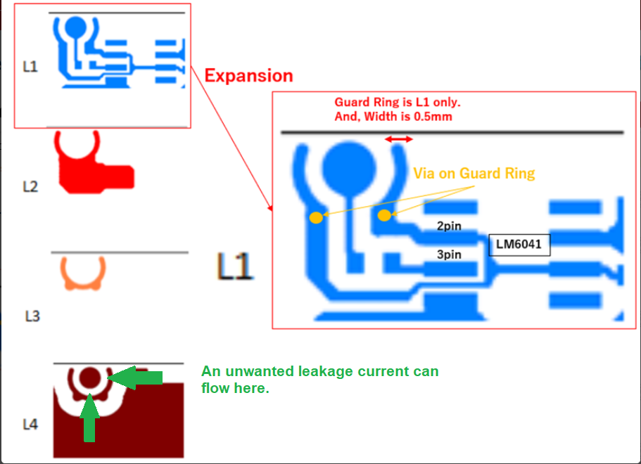
Is there a specification for the position of vias on Guard Ring?

And, can I use it without installing vias?


[Q2]

Is there a recommended pattern width?

For example, could you please let us know the recommended width of Guard Ring in Figure 31?


[Q3]

Due to board limitations, it is not possible to completely enclose with Guard Ring.

So, part of Guard Ring is missing.

In this case, I'm guessing that Guard Ring can't deliver full performance.

Is my understanding correct?


And, are there acceptable criteria for missing Guard Ring?


[Q4]

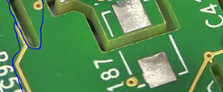
About Figure 35. Air Wiring.

If the environment is hot and humid(so Environments where insulation deteriorates), will the effect of Guard Ring be reduced?

-------


Regards,

Hide

  • Hi Hide,

    Is there a recommended pattern width?

    For example, could you please let us know the recommended width of Guard Ring in Figure 31?

    The holes shown in figure 31 are not necessarily vias but can also be simple holes for through hole components.

    Or do you mean something different?

    Is there a recommended pattern width?

    For example, could you please let us know the recommended width of Guard Ring in Figure 31?

    There's no recommended pattern width. But the width and distance to the neighboured copper tracks should fullfill the requirements of your layout manufacturer. He usually specifies minimum distances and widths. Contact your layout manufacturer.

    Because it's difficult to introduce guard rings on SOIC OPAmps, I would recommend to use the PDIP version.

    Due to board limitations, it is not possible to completely enclose with Guard Ring.

    So, part of Guard Ring is missing.

    In this case, I'm guessing that Guard Ring can't deliver full performance.

    Is my understanding correct?

    If the opening is only small, the guard ring can still be verry effective. But don't route a foreign signal close to the opening.

    And, are there acceptable criteria for missing Guard Ring?

    Good criteria are given in the section "PRINTED-CIRCUIT-BOARD LAYOUT FOR HIGH-IMPEDANCE WORK" of datasheet. But if you are in doubt, only a test layout will give the answer.

    If the environment is hot and humid(so Environments where insulation deteriorates), will the effect of Guard Ring be reduced?

    The idea of using a guard ring is just to help in these situations.

    Kai

  • Hi Hide,

    To add to Kai's comments, below are some additional resources for guarding and explains some other techniques (part 1 and part 3 respectively) that was mentioned in the datasheet: 

    https://www.edn.com/design-femtoampere-circuits-with-low-leakage-part-one/ 

    https://www.edn.com/design-femtoampere-circuits-with-low-leakage-part-2-component-selection/ 

    https://www.edn.com/design-femtoampere-circuits-with-low-leakage-part-3-low-current-design-techniques/ 

    Please let me know if you have further questions.
    Thank you!

    Best Regards,
    Ashley

  • Hi Kai-san, Ashley-san,


    Thank you for the information and comment.

    I have additional question.


    Ashley-san,


    I received questions from our customer.

    May I report Kai-san’s answer as your(TI) answer?


     [Q1_additional]

    I'm sorry for my lack of explanation.

    I would like to know if there are any recommended position of Via(or through hole).

    (For example, A point xx mm away from the +IN terminal etc.)


    I guess that No special regulations.

    However, could you please let us know if you have any information?


    [Q4_additional]

    Kai-san said that “The idea of using a guard ring is just to help in these situations.”

    So, even if the environment is hot and humid(so Environments where insulation deteriorates), Guard Ring can have a good effect.

    Is my understanding correct?


    Regards,

    Hide

  • Hi Hide,

    I would like to know if there are any recommended position of Via(or through hole).

    (For example, A point xx mm away from the +IN terminal etc.)

    The via should not sit too close to the guard ring because some leakage current could dive under the guard ring from the via to the sensitive terminal. Then it's best to have a guard ring not only on only one copper plane but in all planes of the PCB. This would way more effectively shield the sensitive signals from leakage currents originating from the via, if the via sits close to the guard ring.

    So, even if the environment is hot and humid(so Environments where insulation deteriorates), Guard Ring can have a good effect.

    Is my understanding correct?

    Yes.

    Kai

  • Hi Kai-san,

    Thank you for your prompt reply and detail information.

    Ashley-san,


    I received questions from our customer.

    May I report Kai-san’s answer as your(TI) answer?

    Regards,

    Hide

  • Hi Hide-san, 

    Yes, I'm aligned with Kai's recommendations. 

    Best Regards,
    Ashley

  • Hi Ashley-san,

    Thank you for your prompt reply.

    Regards,

    Hide

  • Hi Ashley-san,


    I have additional questions.


    [Q5]

    Our customer use SOIC PKG and 4 layer board.

    And, layout of Guard Ring is layer 1(L1) only.

    Should Guard Ring be placed on all layers?


    [Q6]

    They have a via on top of Guard Ring.

    Could you please let us know if you have any concern?


    <Their Layout image>

    Regards,

    Hide

  • Hi Hide,

    it's still not optimal. An unwanted leakage current can flow trough the FR4 material:

    Kai

  • Hi Kai-san,


    Thank you for your response.


    Could you please let us know if you have any comment for via?


    And, I understand that An unwanted leakage current.

    Could you please let us know improvement if you have any idea?


    Regards,

    Hide

  • Hi Hide,

    Kai is correct regarding leakage through the FR4 material.

    Improvements can be made, but they all depend on the application and required performance.

    when possible, I typically remove the soldermask from the guarded area as this is another source of leakage from the signal to the PCB.

    Creating a via fence can offer additional guarding for the sensitive input, See example:

    This via fence is not a perfect solution, but should slightly reduce leakage through the substrate.

    Alternatively, you can have a slot cut into the board outside the guard ring to physically separate the guarded area from the non-guarded area.

    This will reduce leakage, but typically increases complexity and cost to manufacture:

    Finally, picking a different PCB material can be an effective and simple way to reduce leakage through the substrate. PTFE or ceramic substrates will offer lower leakage than FR4, though cost more to produce. We have used Rogers 4000 series in the past for ultra low leakage PCBs.

    Hopefully this helps a bit in creating your guard structure.

    Best,

    Jacob

  • Hi Kai-san, Jacob-san,

    Thank you for always kind support and comment.

    I greatly appreciate your cooperation.

    Regards,

    Hide