This thread has been locked.

If you have a related question, please click the "Ask a related question" button in the top right corner. The newly created question will be automatically linked to this question.

INA317: INA317 output oscillation

Part Number: INA317
Other Parts Discussed in Thread: OPA317

Hello,

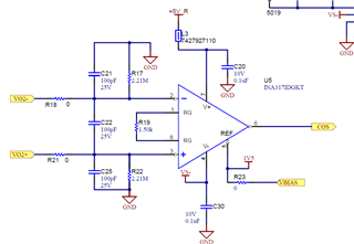
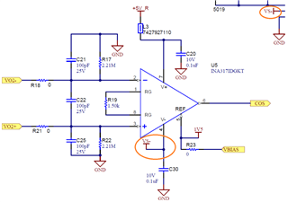
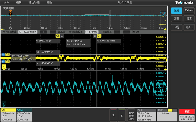
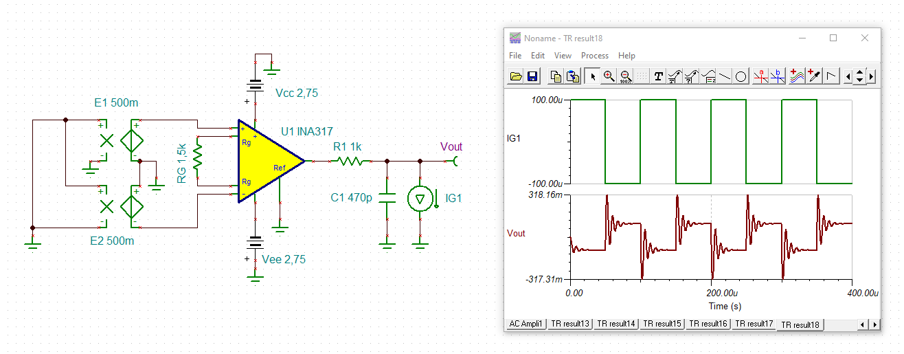
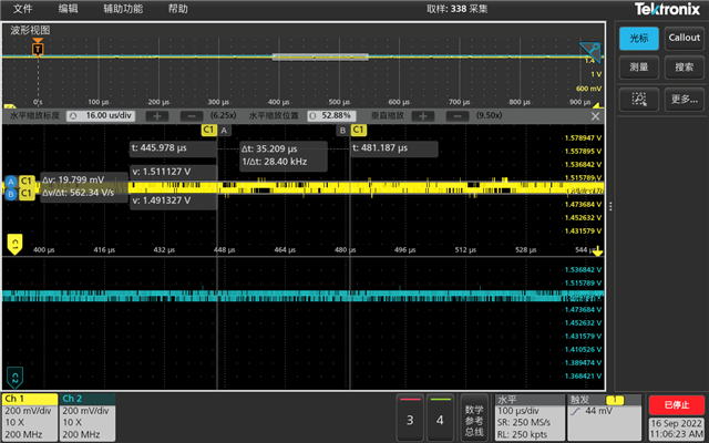
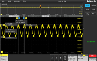
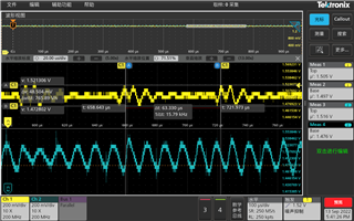
          For the moment, I am debugging the board with INA 317 . I found the INA317 output has some oscillation with 80KHz/80mVpp, see attached:

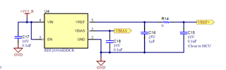
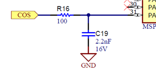
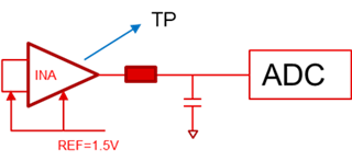
Test condition is: short VO- and VO+ and connect to REF pin from REF2030AIDDCR output (1.5V), INA317 output connect to the ADC input with RC filter (100ohm/2,2nF)

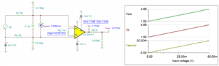
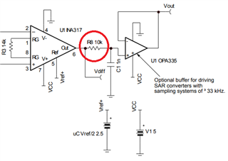
Then I tried something:

  • Remove capacitor between INA input VO- and VO+ ( C22). --> No improvement
  • Reduce the capacitance of ADC external cap (C19) from 2.2nF to 560pF  --> Some improvement, oscillation peak reduced from 80mV to 48mV, Freq changed from 80kHz to 16kHz., below two waveforms are just same capture with different cursor.

  • Then change C19 to 100pF --> got worse. Below two waveforms are just same capture with different horizontal scales.

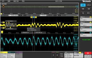
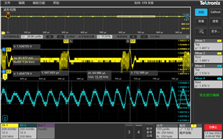
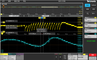
May I have your comments ?  I checked the datasheet that the typical capacitive load drive is 500pF. Is that means we have to use 500pF load for the INA ?

BR,

Chen

  • Hi Chen Gao, 

    Please post the IA's full schematic and tell us about the sensing application. 

    I believed that the RC filter in front of ADC is the charge bucket filter, and its cutoff frequency is fairly high, which means you should not use large capacitor to construct the filter. Please use Larger R and smaller C in values to construct the bucket filter. Larger capacitive load after IA op amp is likely the instability issues. 500pF may be the a typical maximum C_load that INA317 is able to drive at its output without presenting op amp stability issues.

    Best,

    Raymond 

  • Hi Raymond,

        pls find the attachement.

  • Hi Chen Gao, 

    I was hoping to see your input common mode voltage, Vcm, in your front end. Since you did not present it, I am taking a guess. 

    The Gain = 67.67 V/V of the IA, which means that the BW is approx. 4kHz range. The optimum Vcm may be configured near the mid supply or 2.5Vdc for a single supply rail.

    It is not clear what you have. Is VS- is connected to ground or the schematic has dual supply rails?

    I simulated an IA circuit below. I need to know that what is your input signals, sensor's frequency response, Vcm and the excitation voltage, if any. It is possible that the 2.2nf capacitive load may attribute some of instability issue, perhpas there may be some other factors that contributed the oscillation or high output noise as well.   

    From the AC analysis, I did observe a sharp phase change near 80kHz range. If the differential input filter is configured below 4kHz, R16 is increased from 100Ω to ~1kΩ range, 2.2nF is reduced to <500pF, you should not see any oscillatory issues at the output of the circuit.  

    INA317 Oscillation 09142022.TSC

    Enclosed is an image how the differential and common mode LPFs may be configured, also see the reference link below. 

    https://www.ti.com/lit/ug/sbou115c/sbou115c.pdf?ts=1663087419736&ref_url=https%253A%252F%252Fduckduckgo.com%252F

    If you have additional questions, please let us know. 

    Best,

    Raymond

  • Hi Raymond, 

        Thanks for the comment. To answer your question, VS- is connect to GND by jumper. In the schematic, I just provide both single and bipolar power rails solution. For the input signal, I just short the VO2- and VO2 + together then connect to the REF pin with 1.5V supply like the block diagram I post previously. So the output of INA is also a DC. I will try adjusting the input/output filter to see if any improvement. 

    BR,

    Chen

  • Hi Chen Gao,

    For the input signal, I just short the VO2- and VO2 + together then connect to the REF pin with 1.5V supply like the block diagram I post previously.

    You are unable to short the input together without any input common mode voltage, since you are using a single supply rail. Please short both input and attached to 2.5Vdc, where Vcm = 2.5Vdc. 

    By shorting the input, Vcm is operating below the turquoise color rectangular, which is not linear part of IA response. The input is a difference of VO2+ and VO2- on top of Vcm mode.  

    If you have additional questions, please let us know. 

    Best,

    Raymond

  • Hi Raymond,

         Vcm is 1.5V which is same as REF pin since they are connected together. Anyway, I have also tried 2.5V Vcm connected to the input of INA and the noise still comes.

          I modified ADC external input RC with 1kohm/470pF. Pls find below waveform ( yellow curve), oscillation peak reduced from 80mVpp to 40mV , oscillation frequency ramp up to 200kHz instead of 80kHz, oscillation repeat period = 16kHz. 


  • Hi Chen,

    don't forget that the INA317 is a very low power instrumentation amplifier drawing only 50µA supply current. Such a instrumenation amplifier cannot easily drive a dynamic load like an ADC like a normal instrumenation amplifier drawing a much higher supply current:

    You can see this from the huge settling time and the ultra low slew rate of INA317. You will need to add a buffer to drive the ADC as shown in figure 41 of datasheet.

    Kai

  • Hi Chen Gao, 

    Kai has a good point. Please increase the output series resistor to 5kΩ-10kΩ range and see if it is still oscillating. Adding a buffer will ease of loading on INA317. 

    Best,

    Raymond

  • Sorry, I forgot to attach the sim file:

    chen_ina317.TSC

    Kai

  • Hi Kai,

        Actually for my testing, I did not run the ADC sampling which means the load of INA317 is only 1kohm / 470pF. I monitored the oscillation by oscilloscope on the output. 

  • Hi Chen Gao, 

    The issues are Riso is still too small to compensate the pole generated by (Zo + Riso) with 470pF capacitive load. I thought that Riso = 1kΩ is large enough to compensate the pole, but it did not as shown in the simulation below. I assumed OPA317 is used in the last stage of the IA, but it is likely not the case.  In any case, there is not enough phase margin, hence you see the oscillation at the output of INA317. 

    If I have a model that is used in the last stage of INA317 IA, the conclusion will be the same.  

    INA3 17 3rd op amp w OPA317 09152022 - autosave 22-09-15 19_33.TSC

    If Riso is increased from 1kΩ to 5kΩ as the example below, the phase margin is increased from 25 degree to approx. 55 degree. Since the simulation may not reflect to the actual INA317 used inside of the IC, it may not provide you with the actual desired outcomes. However, the direction of increased Riso at the output is correct.  

    Regarding to this part of op amp compensation approaches, please visit PRAMPS training video below. It provides the theory and method how to compensate an op amp when driving a capacitive load.  

    https://training.ti.com/ti-precision-labs-op-amps-stability-capacitive-loads?context=1139747-1139745-14685-1138805-13952

    Best,

    Raymond

  • Thanks Raymond, I tried 10kohm Riso and the oscillation was gone but actually such big resistance will impact my ADCs min sampling time especially oversampling is implemented. So additional OPA is needed I think. 

    .

  • Hi Chen,

    but actually such big resistance will impact my ADCs min sampling time especially oversampling is implemented. So additional OPA is needed I think.

    Exactly.

    Kai