This thread has been locked.

If you have a related question, please click the "Ask a related question" button in the top right corner. The newly created question will be automatically linked to this question.

THS4541-Q1: FDA different input signal common mode and amplitude

Part Number: THS4541-Q1
Other Parts Discussed in Thread: THS4551

Hello,

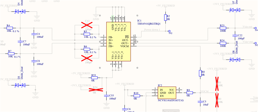
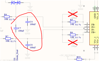
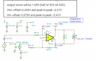
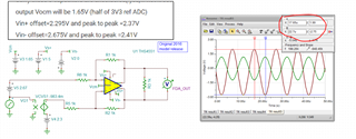
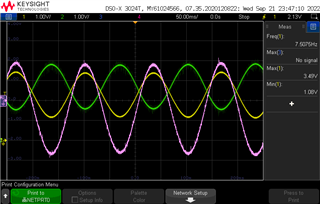
I am using a TI FDA ( ref in the title) to amplify a sensor  providing a sin+/sin- output. I originally thought both input signal would have the same Vicm of 2.5V and same amplitude with opposite phase but it's not the case( see picture).

The problem is now the FDA output are not symmetrical around Vocm. Does FDA can work with such input with different Vin common mode and different amplitude?

yellow Vin+, green Vin-

math =yellow-green (1V/div), not centred around zero.

Thanks,

Clement

  • Hi Clement,

    please post a schematic.

    Kai

  • Well the FDA can do a lot of things, and may well handle your situation - again a schematic would be necessary, but you might read this as well, the 2nd half of this covers FDA's and of course a TINA file will tell you (and us) a lot. 

    https://www.planetanalog.com/input-and-output-voltage-range-issues-for-high-speed-cfas-and-fdas-insight-2/

  • Hi, in the schematic there is a gain of 1.4( 1.4 was ok when both Vin+/Vin- had an offset of 2.5), I reduced the gain to 1 to avoid to saturate the output( since Vin+/Vin- offset are more 2.3/2.7V).

    Since from a sensor to another the sensor output offset will change, it can saturate again.

    I don't think there is way to keep only the differential part of the input signal without bother to much of the offset of each input( provided FDA Vin_cm is in the good range) and to have a clean FDA output center on Vocm?

  • Well 1st Clement, you need to get rid of those 100nF on the summing junctions, that is a path to oscillation by themselves, Can you list the two input common mode and Vpp and the output desired Vocm. 

  • Sorry these 3 capacitors are unsoldered( yes, if not it oscillates)

    output Vocm will be 1.65V (half of 3V3 ref ADC)

    Vin+ offset=2.295V and peak to peak =2.37V

    Vin- offset=2.675V and peak to peak =2.41V

  • Ok Clement, I set this up with the lower speed and power THS4551, probably plenty fast for your needs - also, those R's are too high for parts this fast, I went ot 1k and 1k for gain of 1, a gain of 1.4k did in fact show non-linearity in the transient, but the gain of 1 works ok I suppose, 

    1st, the DC operating points, clearly with a 2.675-2.295 = 380mV output offset (gain of 1) - and that is what we get, 

    Then if we turn on the sine wave sources (I used a dependent source to get the inverted attenuated version on the V+ side from the V- side) we will get an offset sine wave at the outputs. That Vpp is just the sum of the two input Vpp shifted by that same initial 380mV due to the DC input levels. This is a 100kHz input, 

    File attached, 

    THS4551 version.TSC

  • Hi Michael, thanks, I have also the same results.

    My sensor works at low frequencies ,it's why I use higher resistance value. To be honest I think to use a FDA is slightly too expensive for this low frequency application.

    I just wanted to have 2 sin+/sin- input  converted to a differential signal centred around 1.65V for the ADC. Maybe I can use 2 classic op amp.