This thread has been locked.

If you have a related question, please click the "Ask a related question" button in the top right corner. The newly created question will be automatically linked to this question.

INA849: Dc servo on real pcb is not working as like in simulation, bug with INA846 or THP210 in Tina?

Part Number: INA849
Other Parts Discussed in Thread: THP210, , TLV2186, OPA333, OPA1637, TINA-TI

Hello,

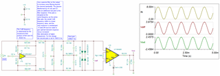
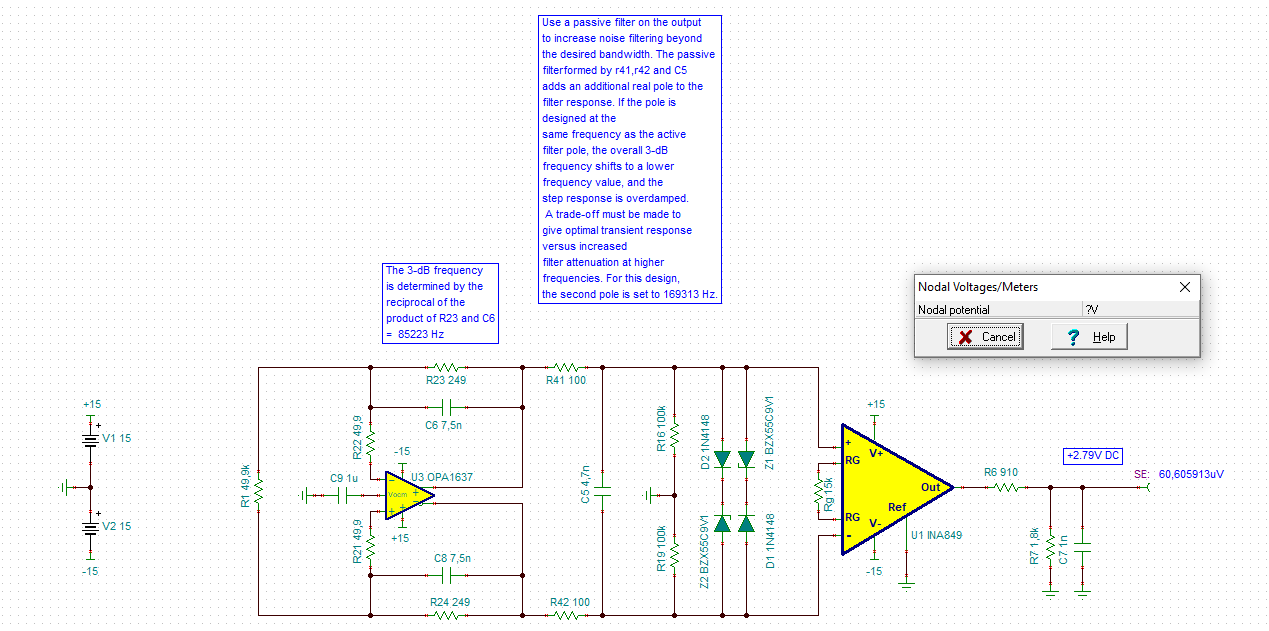
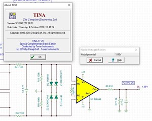
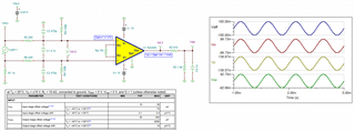
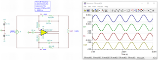
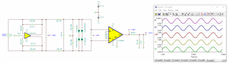
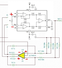
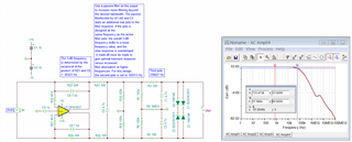
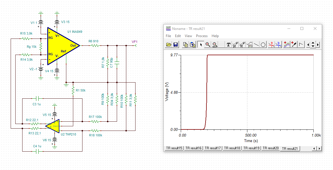
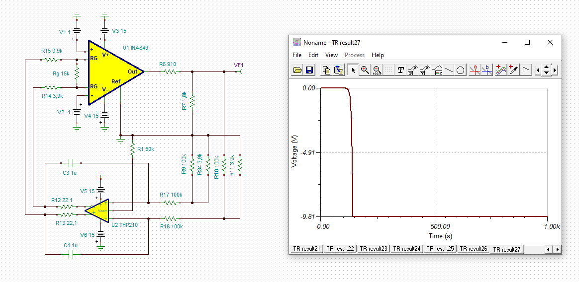
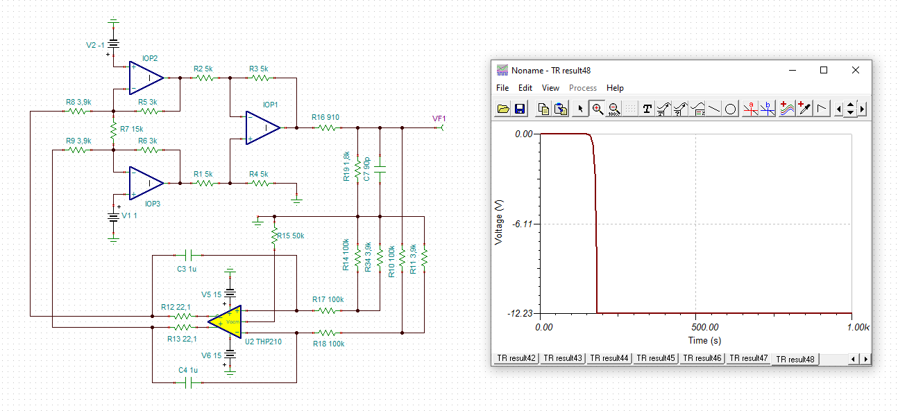
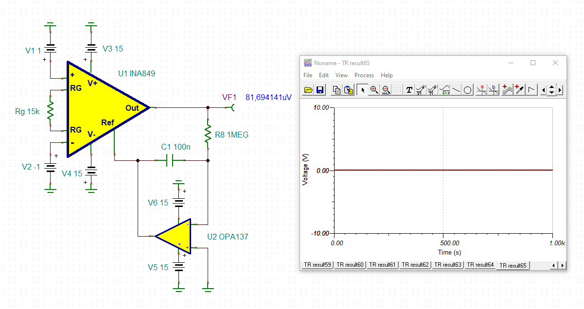
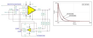
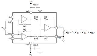
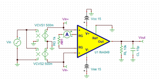
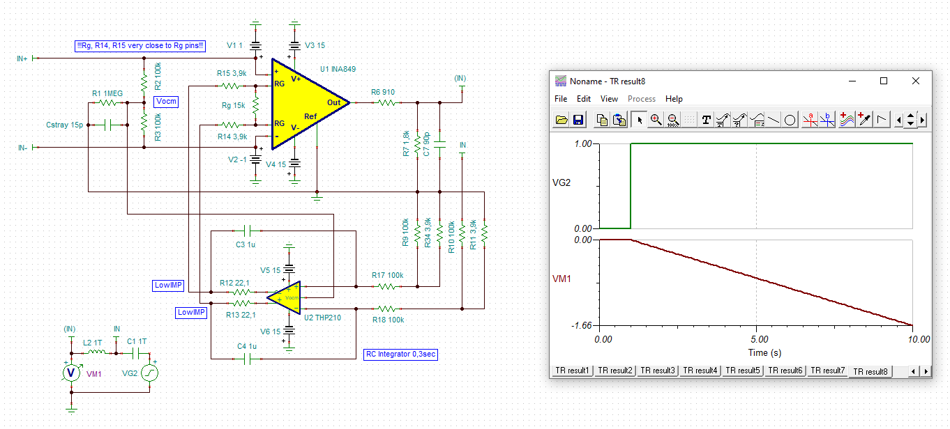
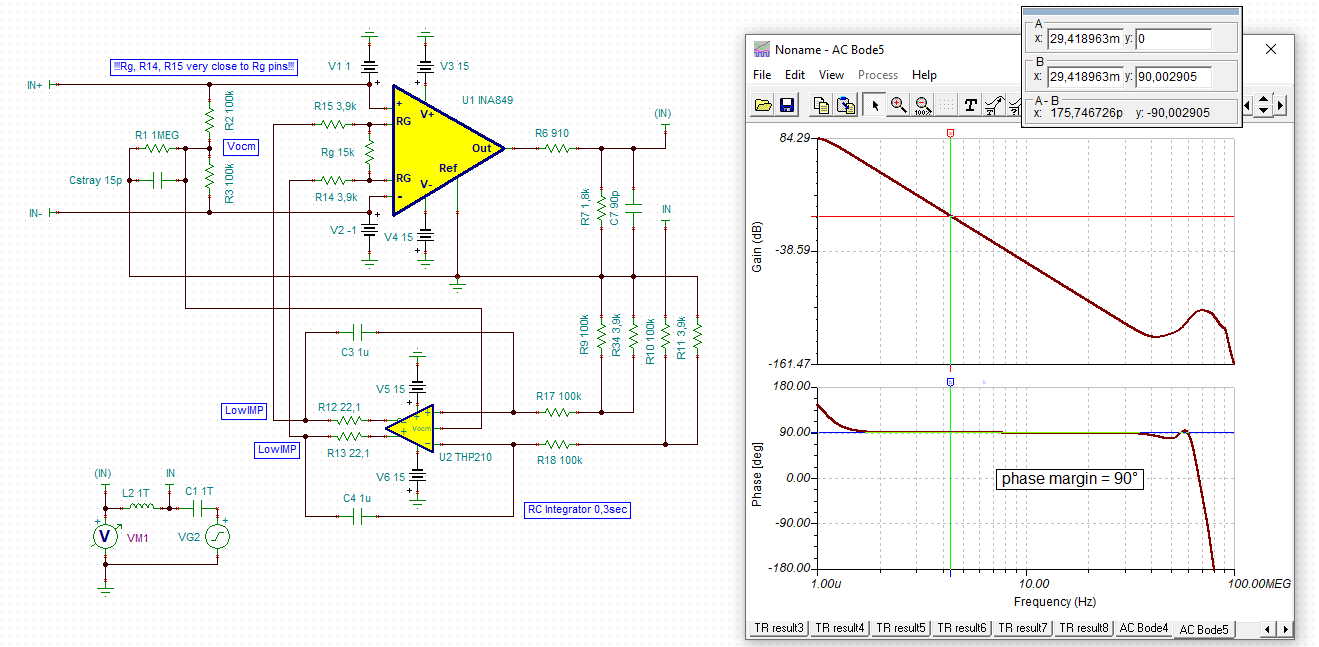
I have problem with DC servo, in Tina simulation everything is working correctly buton real world I have DC fully to the rails on INA RG pins and half of that at negative DC at the INA output!! That happen starting wrom DC null volts and after 10-20 secconds fully to the rails! Can you please tell me maybe RG pins on INA have somehow wrong + and - in sim model? Or maybe THP210 have wrong + and -  in sim model? Here is my simulation. Thank you for any information regarding this isue wFullyDIFF I-V INA849 DCservo.TSCith DC servo!

  • On real model mean on my real pcb which is identic to schematic from simulation attached above, I have +-15V at RG pins and -8.5V at INA849 out on resistor R6 which is indication that DC servo is not working! But on Tina simulation attached above everuthing is right. Thank you for help!

  • Hi Jimbo,

    why so complicated? Why not inserting the DC servo into the REF pin of INA849?

    Also, the RG pins are very sensitive to EMI and don't like any stray capacitance. I would only connect the gain setting resistor to the RG pins, nothing more.

    Kai

  • Hi Jimbo,

    I agree with Kai's recommendation. 

    Please simplify the Rg gain settings for the application. Below is an example. 

    INA849 Input mod 12242022.TSC

    If you have additional questions, please let us know. 

    Best,

    Raymond

  • Thank You so much!

  • Is this circuit ok? Thank You so much!

    dc_servo.TSC

  • Hi Jimbo,

    I see that you like to use our full differential op amplifier, and we are very appreciative. 

    The Vref input requirement is a low impedance source, which means that it may be a voltage source that is capable to source and sink (Vref bandgap) or output of precision op amp. 

    Our bandgap reference options are: REF02, REF3425Q1, REF31XX, REF4132, REF50XX or REF60XX etc..  

    Since you need -2.7856Vref for the level shift, here is an example. The Vref op amp is OPAx186 or TLV2186 or OPA333 zero-drift op amp. 

    INA849 with Ref -2p7856V.TSC

    If you have additional questions, please let us know. 

    Best,

    Raymond

  • Thank you! But this is much complicated than circuit from the main thread, is not?  RG pin in FullyDIFF I-V INA849 DCservo.TSC have GND reference, and THP210 driving RG pins, it is very good on simulation but on real world its seems wrong polarity on INA849 RG pins or wrong polarity on THP210 out pins?? Since it pump DC in vicewersa for about ten secconds to the full rail voltage, than I have +-15V on RG resistors pre RG pins and I have -8.5V at INA out, can that be bug in sim model of the THP or INA?

  • Gnd in this case is masterGnd for whole preamp circuit.

  • Sorry, mean REF pin of the INA is master GND

  • Hi Jimbo,

    I'm a bit confused right now. What do you need the DC servo for at all?

    Kai

  • I want to remove any DC from the out of the INA, to have DC free on bandaxal. I know I can put bipolar condensator at the out of INa but  Iwould be happy to have no condensator at all! Can you please take a look at picture, this is real measurement on real model! As you can see when R14 and R15 is removed, dc servo have no function, INA ref pin is refered to GND, zero volts is measured at INA out! But now take a look at simulation, notice 2.79 DC at out, thats indication that something is not ok in simulation since on real pcb measured zero volts but on simulation +2.79V !

    INA849_2.79.DC.at.OUT.TSC

  • When I put back r14 and r15 DC on those resistors start from null volts and linearly slovly getting to the rails volts it happen cca after ~10 secconds, and INA out produce -8.5V, that's reason for my post here. On simulation model things is totaly diferent, no problem at all. Bug in INA or THP model? I'm believing THP out pins have wrong polarity or RG pins on INA have wrong polarity? Simulation tells no changes at all when I revert polarity on booth.

  • Hi Jimbo,

    with the 49k9 dummy resistor I get 61µV:

    Kai

  • Might be Tina version related? Please see picture, measured again and I have +1.85V at SE but +2.79V at R6. Whats say whole circuit from the first post? How can be explained ultra high voltages on RG pins, might be wrong plarity THP out or RG on INA or something else? I realy have no idea, its totaly two diferent measurements real pcb<->simulation, now your simulation even make diferent result :( Preamp have great sound but with dc servo removed and insterted condensator between R6 and the rest of components, I'm realy very interested to make servo from the first post working, or tat least to get idea what is wrong there, I suspect wrong polarity on INA or THP, but seems its not possible to figure out or sim? Thank you so much!

  • Hi Jimbo,

    I do not see any issues with Tina tools. We are using the same Tina revision as yours. 

    The INA849's transfer function is:  Vp = Gain * Vin + Vref + Voffset. And the circuit is simulation correctly. Kai demonstrated the same thing.  

    For instance, at Vin_pk = 99.73mV, Vp = 1.4 V/V * 99.73mVpk + 0 = 139.622 mVpk. The model is simulated approx. 139.67mV, which includes small Voffset. 

    INA849 Input Sim 10272022.TSC

    With the constant current source of 4mA at 1kHz, I am not certain what you are trying to do. This is not a typical FDA differential input circuit, see 4mA current loop around the OPA1637. With 4mA, 1kHz input, the output Vdiff swings from 0 to 3.98Vpk. 2 * 4mA*249Ω = 1.992Vdc; and this is the differential input voltage across INA849's input (this is NOT common mode voltage across the INA849's input). 

    OPA1637 Analog input 10272022.TSC

    With the differential input of Vin = 1.99V, Vp = 1.4 * 1.99 + 0 = 2.786 Vdc, which is exactly the simulation is shown. 

    If you have additional questions, please let us know. 

    Best,

    Raymond

  • Hi thank you! To explain in details about whole diy device. Four mA at the imput is from diy DSD current mode 32 steps moving average discrete dac, this is schematic for dac:

    DSC252.pdf

    If you take a look into dac schematic you should notice diferential current at the output, curently it is more than 10mA so we added two resistors 470 ohm to lover mA to ~8mA per rail, next what we wanted to do was to replace audio transformers with opamp based circuit, we chosed INA849 as its currently the best one for diff to se. First stage is i/v and we used diferential Opa1637, next we converted diff to se with Ina than the rest of circuity, multi fb low pass filter, bandaxal and finaly se to diff at the out. Whole circuity is frontend for Hypex UCD180HxR class D power amplifier. It working very good curently with this circuity:

    FullyDIFF I-V INA849.TSC

    But thats not the same as first concept wit THP210 as a dc servo since now we have condensator after Ina output. First circuity which we designed working good on simulation and it is:

    7450.FullyDIFF I-V INA849 DCservo.TSC

    But its not working on real bcb! On reall pcb we have +-15V at RG pind which is totaly diferent than in simulation! What we want to figure out is why we have big deviation between simulation and real pcb!? In simulation we 567uV at INA output but on real simulation we have -8.25V !! In simulation on RG pins we have ~+-990mV, on real pcb we have +-15V !! THats big diferencie. Again, whole circuit is working if we remove r14 and r15 and add condensator bitween ina out and the rest of circuity but thats not a goal, goal is to have dc servo to remove any DC at Ina output. So question is why we have big deviation between simulation and real pcb? THank you so much!

  • Hi Jimbo,

    I have the TINA-TI Version 9.3.150.4.

    TINA-TI has the nasty tendency of self-damaging its simulation file after some runs. I give you an example: It happens to me very often that I start with a correct simulation file and everthiny is doing well when running the first simulations. But when I change the component values and parameters of voltage or current generators during the optimization process afterwards something strange can happen: When I get an error message later for any reason and change all the component values and parameters back to the inital values -where the simulation did still run correctly-, the simulation does no longer run correctly but I now get error messages. TINA-TI has definitely altered the simulation file in the meantime for any reason. Any further simulations become senseless then because TINA-TI behaves weird from this moment on.

    The only remedy then is to draw a new and fresh schermatic again by importing fresh components and chips. Do not copy and paste anyhing from the damaged simulation file into the new schematic.

    Another tipp I can give you is to not put too many components and chips into one simulation. The run time and the simulation problems grow exponentially.

    Kai

  • But its seems FullyDIFF I-V INA849 DCservo.TSC is not damaged yet, if you draw new one you will get excatly the same result. Problem is that on real pcb on RG pins we have DC about null, after ten seccons we have +-15V linearly from zero volts, which might be wrong polarity on RG pins of INA849 or wrong polarity of THP210 out pins? Can this behavieor can be simulated on Tina? Or do you have idea what is wrong on real pcb? It looks like vicewersa, istead of to remove DC it pump DC to the rail voltage, which might be that one of pins is wired incorectly e.g. inverting/noninverting pins need to be vicewersa. Thats why I opened this thread in hope somebody figure out isue.

  • Can Tina run circuity from the first post for about 10-20 seccond? Thats way we will be abble to imitate real pcb behavior with vicewersa efect of the dc servo.

  • Hi Jimbo,

    ok, then divide and conquer! Make the following modifcations in your "real world" circuit:

    1. Remove U4, U5 and U6 from the circuit. (Make a cut left of R27 and remove the supply voltages to all of these OPAmps so that these three OPAmps are no longer existent in your circuit.) Do you still see a run away?

    2. Connect the Vocm input of U2 to signal ground instead of R1, R2 and R4. Do you still see a run away?

    3. Increase R14 and R15 by a factor ot ten. Do you still see a run away?

    4. Then remove U3 and all the other components from the two inputs of INA849 from the circuit. Instead connect +1.0V to the +input of INA849 and -1.0V to the -input of INA849. Do you still see a run away?

    Kai

  • Hi, one questing trought, is polarity connections ok here? 

  • Hi Jimbo, 

    I'd like Kai's plan and it may locate the issues sooner than other approaches. 

    In your input front end, I ran the overall AC filter response (common mode filtering ~(R23 + R41 + R3)||C1) = 75.4kHz and differential mode ~2*(R3 + R41)||C5 = 48.5kHz filtering);  and the circuit's common mode filtering is placed too close to the differential mode filtering. Normally, you'd like to place the common mode filtering at least a decade after the differential mode filtering. This will prevent the common mode noises convert into the differential mode signals, since the capacitors may have tolerance issues up to +/-20%.   

    Below is the input filter configuration for the instrumentation amplifier. 

    https://www.ti.com/lit/ug/sbou115c/sbou115c.pdf?ts=1666973123425&ref_url=https%253A%252F%252Fwww.ti.com%252Ftool%252FINA826EVM

    If you have additional questions, please let us know. 

    Best,

    Raymond

  • jimbo_ina849.TSC

    And after remove of C7:

    Haven't I told you to not put too many devices into one simulation??

    Kai

  • And with an ideal differential amplifier:

    jimbo_ina849_2.TSC

    Kai

  • And with a standard DC servo:

    jimbo_ina849_4.TSC

    Kai

  • Hmm thank you so much, Kal gaved good simulation which confirms vicewersa efect of the dc servo made by thp210, but I see only one strange thing there, c7 iz like an parasite cap of the 90pF, how is that possible that you now have vicewersa polarity of the DC at Ina out, is not that strange??

  • One more thing, seems INA have wrong polarity indeed, see behavior on ideal diff opamp!!

  • Hi,

    Kai schematic in which he proves the error of the DC output offset in POS and in NEG (when you desolder C7 output filtering against peaking at high freq, you also have that in DS succinctly tried/described)

    In the same schematic, I just turned R14 and R15 (criss-cross Rg pins at INA849) and ....look, it works as it should work!!! :)

    The input has a differential of 1V and -1V DC offset, (as posted by @Kai)
     
    In StartUP (see graph), that DC offset on the INA849 rises/builds (depending on the polarization at the inputs +IN and -IN) and jumps over 2.5V, after the RC constant of the diff.Integrator around 2.5... 2.6sec, which can be seen in the graph of StartUP (we chose a slow Integrator so that there is no impact in the Audio area, that's completely OK), the DCoffset present at the input begins to correct, the Slope is slow because we already have such an RC constant... in the end it succeeds and to completely correct,  and what is more important to keep it at the output of INA849 and nulled!

    P.S The RC integrator constant is about 3sec or that 0.3Hz, marked by an error in the scheme...it was in a hurry!

    Well, maybe you should revise the INA849 macro model?

    Thank you so much!

  • Hi Jack, Kai,

    Cool circuit, this is very useful for high-gain AC circuits that otherwise would have limited common mode range due to offset errors.

    But, I don't think the polarity is wrong for the RG pin connection; the RG pin is located to the corresponding amplifier that the internal feedback resistor is connected to, similar to our INAs:

    The block diagram above shows the inverting terminal above the non-inverting terminal, whereas the TINA model shows it the other way around.

    Due to the definition of the polarity, a positive voltage on the non-inverting terminal would result in a positive voltage on that amplifier's output.  This means that current will flow OUT of the RG pin associated with the positive input.  For sanity's sake, I checked this, and it does appear to be the case:

    As far as the way that the circuit is connected, I also thought the same way;  I assumed that in order to cancel the voltage on RG, the feedback servo amplifier had to be inverting from the output relative to the RG pin.  But, as it happens, this is not the case, because what we are effectively trying to do is make the input of the internal diff. amp zero, not the voltage on RG.  Actually, the voltage on RG needs to match the input voltage, and the FDA needs to deliver enough current to INVERT the output of the (input) amplifier.  So, in order to make the input to the diff. amp. zero, there must be current flowing INTO the RG pin on the positive amplifier.  I believe the very busy simulation below proves this:

    Note current flows INTO RG on the positive side, and must flow out of RG on the negative side.

    Agreed?

    Regards,
    Mike

  • HI,

    yes, I'm tested on real pcb like this jimbo_ina849 popravljeno RG pins.TSC and I can confirm things work now! Thank you so much!

  • Hi Michael,

    yes, agreed. Another method is to open the feedback loop and add a stimulus to see the step response: To provide a stabilizing negative feedback "VG2" and "VM1" must show signals of different polarity, which is the case in the circuit below:

    jimbo_ina849_5.TSC

    And with the same method we can determine the phase margin of the DC servo:

    So the DC servo is stable.

    Kai