This thread has been locked.

If you have a related question, please click the "Ask a related question" button in the top right corner. The newly created question will be automatically linked to this question.

OPA3S328EVM: Build a Programmable Gain Transimpedance Amplifier

Part Number: OPA3S328EVM
Other Parts Discussed in Thread: OPA3S328, TINA-TI, ADS1675, LMP7721, LMP7715

Hello Experts,

Our customer has a technical question about the product OPA3S328EVM.

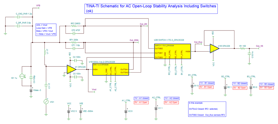
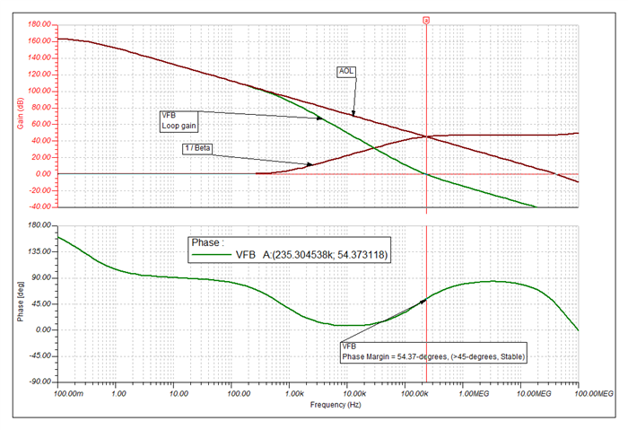
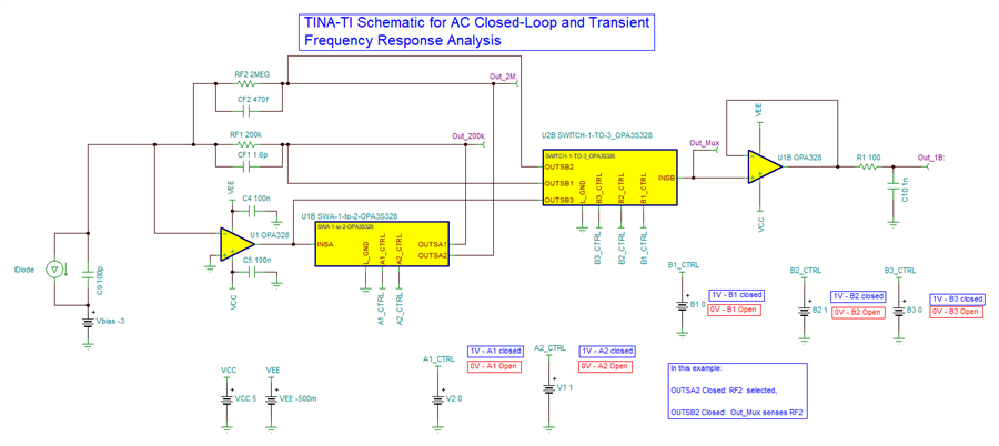
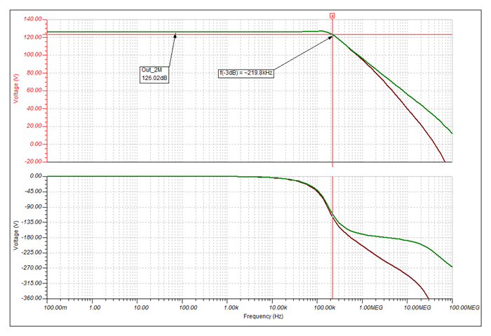
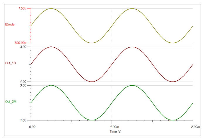
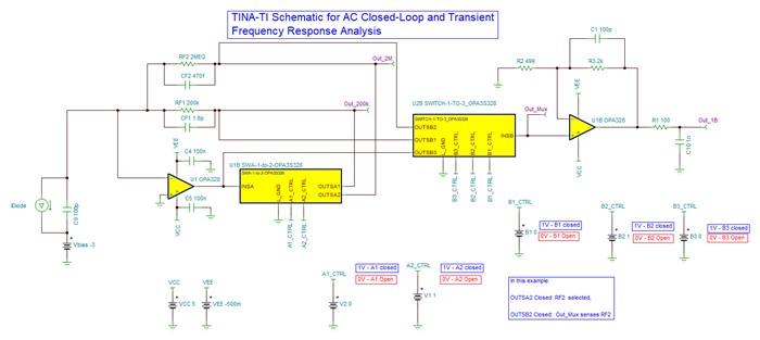
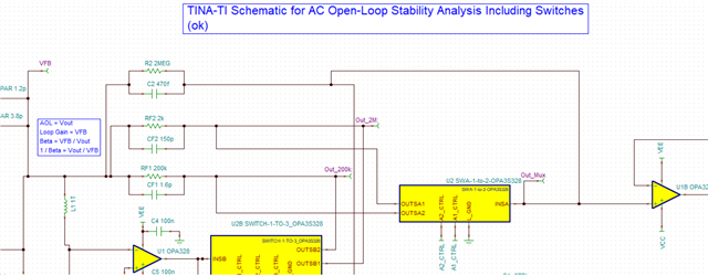
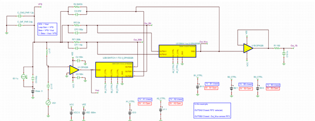
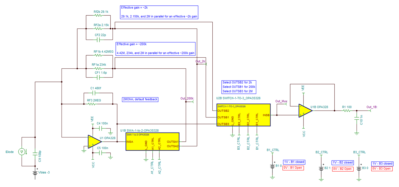
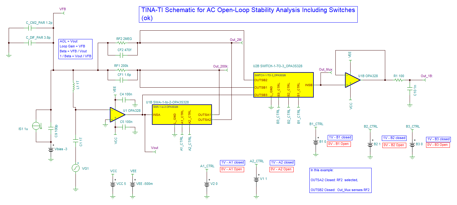
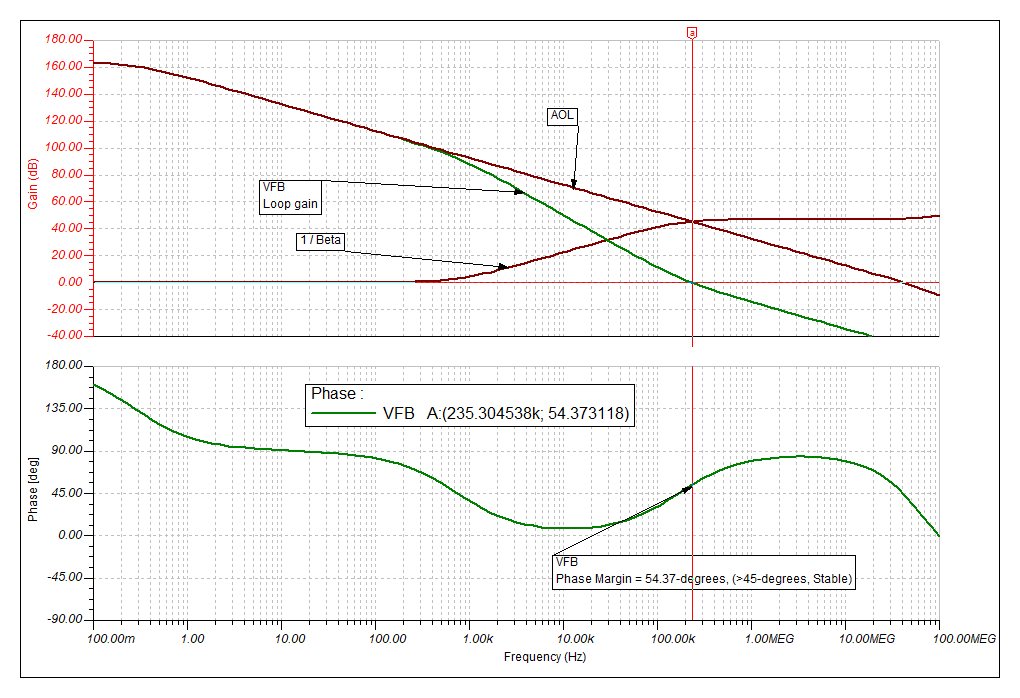
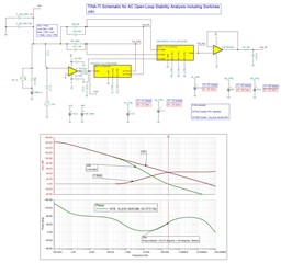
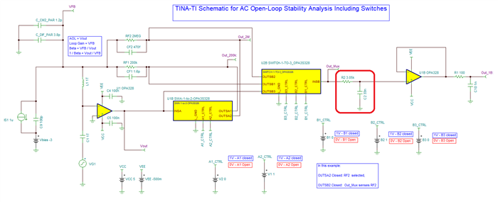
He has been going through the "Application Report: Build a Programmable Gain Transimpedance Amplifier Using the OPA3S328" and he is curious if we have tested the TIA with larger feedback resistors (~10s of Mega Ohms). The report only talks of feedback /gain of 200kV/I but not any larger. 

In addition, can the customer get a spice netlist for the evaluation board? The customer already has the spice model for the TIA, obtained it from TI website. I mean the OPA3S328EVM

I hope you can help us. Thank you.

Best regards,

Gerald

  • Hello Gerald,

    The OPA3S328 PSPICE (and TINA-TI SPICE) macro-model currently posted in the web is currently in the queue to be revised. The op-amp block (OPAx328) works without issues, but the switch block/circuit can exhibit issues converging in TINA, and in some cases, issues converging on PSPICE on certain conditions.  The issue is in the modeling team’s queue to be fixed. 

    In the interim, I am providing a temporary model, using the same approach documented on the App. Note: Build a Programmable Gain TIA Using the OPA3S328.  The temporary model uses the same OPAx328 block with the complete op-amp specification (includes AOL, output impedance over frequency, noise, offset and input/output range limits, etc.) However, for now, we use a simplified switch model, it models the typical parasitic resistance and capacitance on the switch (RON, CIN and COUT).  This provides a good first order approximation to check stability, bandwidth and noise on the TIA circuit.

    Attached is a TINA-TI simulation example, showing the circuit configuration shown on Site 1 of the OPA3S328EVM, but modified for a 2MΩ feedback resistor, and assuming a photodiode with capacitance of ~100pF.  Using Equation 8, of the OPA3S328 Application Note, with RF=2MOhm, FGBW=40MHz and assuming a total input capacitance of 105pF, provides a starting point or estimate of the minimum feedback capacitance at CF>~470fF. (Edit, 11-09-22: Corrected error, RF=2MOhm on simulations below)

    AC open loop stability analysis example on TINA-TI:

     The simulation below shows the AC open loop stability analysis showing the circuit is stable, with 54-degrees of phase margin.

    TINA Open-Loop AC Stability Analysis File (Example):

    OPA3S328_2Mohm_open_loop_stability_example_k.TSC

    Closed-loop circuit transient and AC frequency response example on TINA-TI:

     The simulation shows the closed-loop circuit transient and AC frequency response, where the 2MOhm TIA has a bandwidth of about 219kHz:

     TINA Closed-Loop Transient and AC frequency response File:

    OPA3S328_2Mohm_closed_loop_example_keep.TSC

    The simulation files attached can be used as a starting point and modified per your TIA gain/BW requirements and photodiode model/bias conditions.

    Please let me know if you have questions.

    Thank you and Regards,

    Luis 

  • Hello Gerald,

    The example above uses a gain of 2-MOhm, where depending on the TIA closed-loop bandwidth requirement, the compensation capacitor may be quite small; and the circuit will become sensitive to stray capacitances. 

    If the application requires gain in the 10s MΩ, depending on your bandwidth requirements, another approach is to use additional gain on the second stage, for example, using G=+5V/V as shown below:

    Thank you and Regards,

    Luis 

  • Hi Luis

    I will be using OPA3S328 RGR (20-Pin VQFN) package. I want to program TIA with 3 feedback gains (attached) using OUTSB1, OUTSB2, OUTSB3 pins. My gain will be 2 Mohm, 200kohm, and 2k ohm. As mentioned in the application note we will not have any significant gain error (<0.06%) in high-resistance feedback path however with low resistance feedback path this gain error will increase to 6%.

    For highly precise current measurement I want to do the following:

    1. Opamp B with 3 integrated switches for current sensing of 0.1nA to 5mA with three feedback gain (2 Mohm, 200kohm, 2kohm).
    2. Kelvin probe accurate resistance measurement for low resistive gain (200kohm and 2kohm) feedback path using Opamp A having two integrated switches.
    3. Can we connect the OUTSB3 (2Mohm) path directly to the Non-inverting terminal of Opamp A? Will it induce any interference in measurement as output to 2:1 MUX will be in a floating condition (SELA1 = High, SELA0 = Low).
    4. In practice, what happens if we measure the photodiode current more than the Quiescent current. For eg can we measure 10 mA current accurately with part where spec sheet say it has Quiescent current of 3.8 mA/channel.
    5. Vsupply+ = 1.5V, Vsupply- = -3.5, INB+ = GND (cannot pull to positive voltage due to device physics constraints). Can we utilize the Opamp A here for “buffer and positive level shifting” so that it can be cascaded to unipolar differential ADC (ADS1675, Input range 0 to 3.5V)?

    Kindly correct me for the necessary modifications.

    Thanks

    Deepak

  • Hi Deepak,

    Is this the same project described on Gerald's post above, or are these questions referring to a different project? 

    As you correctly have mentioned, the OPA3S328 on the QFN package offers a 1-to-2 switch matrix and a 1-to-3 switch matrix; hence, the QFN package option is limited to perform a true Kelvin sense connection on two TIA gains.  The datasheet mentions an upcoming DSBGA YBJ package version (24-pin) on development that will include two, 1-to-3 switches, but this is upcoming and not yet available.

    Regarding your questions:

    Can we connect the OUTSB3 (2Mohm) path directly to the Non-inverting terminal of Opamp A? Will it induce any interference in measurement as output to 2:1 MUX will be in a floating condition (SELA1 = High, SELA0 = Low)

    If you need 3 gains: 2-Mohm, 200-kohm, 2-kohm, using the available VQFN OPA3S328 device with the 1-to-2 switch matrix and a 1-to-3 switch matrix, I would recommend you leave as default the 2-MOhm resistor on the feedback. Please refer to one possible circuit below.

    Edit: 11/14/22: Revised the resistor feedback values.

    - For Case (A), by opening the OUTSA1 and OUTSA2, the switches on the TIA stage, you have the default RF3, 2-MΩ gain.  Use the OUTSB3 to sense the 2MΩ gain directly.

    - For Case (B), close OUTSA1, open OUTSA2 you can have set of parallel a feedback resistors RF1a, RF1b=234kΩ || 4.42MΩ, where the default feedback RF3 2-MΩ, in parallel combination of RF1a,b and RF3 forms a value nominal very close to ~200kΩ. Use the OUTSB1 switch to sense in close proximity to the point where the RF1a, RF1b resistor terminals connect.

    - For Case (C), close OUTSA2, open OUTSA1, you then have the RF2a,b=29.1kΩ||2.15kΩ, combination, where RF2a,b in parallel with the default feedback RF3=2MΩ forms a value nominal very close to ~2kΩ. Use the OUTSB2 switch to sense in close proximity to the point where the RF2a, RF2b resistor terminals connect.

    There will of course a subtle gain error on cases (B) and (C), since in reality you don't have an exact 2-MΩ resistor in parallel, but actually the series combination of 2-MΩ + switch RON resistance. Nevertheless, given that RON is in the range of ~125Ω range or less, the error is small compared to  2-MΩ resistor (less than 0.06% gain error in this specific example). 

    In practice, what happens if we measure the photodiode current more than the Quiescent current. For eg can we measure 10 mA current accurately with part where spec sheet say it has Quiescent current of 3.8 mA/channel.

    The TIA capability to support a large photodiode current is primarily limited by the output stage current drive of the transimpedance amplifier.  Also, you need to consider the output voltage range swing limitations, and voltage supplies of the amplifier.

    The OPA3S328 output can sink and source -68mA and +63-mA typical respectively (note this is the typical spec, and there is variation on the output current limit). Hence, the supported photodiode current has to be well below the current drive limitation. Therefore, in this case, the OPA3S328 is able to handle 10mA from the current output drive perspective without issue.

    However, you need to carefully consider the amplifier voltage output swing range limitations. The amplifier requires an amount of headroom from the supply rails. Please refer to figures 6-20 to 6-23, "Output Voltage Swing vs Output Current" on page 12 of the OPA3S328 datasheet.   

    If you need to support ~10mA diode current, then the minimum 2kOhm gain will not work as you will rail the TIA output, with a large voltage: (2kOhm+RON)*10mA=>20V, which is not possible.   I recommend reducing the smallest TIA gain resistor option, to bring the output voltage range within range of the TIA amplifier output swing, considering the switch resistance, and output swing range limitation of the amplifier. If you need more information, please provide a schematic showing the potential of the TIA non-inverting terminal, and how the photodiode is biased and the polarity of the photodiode as it is connected to the TIA input.

    Vsupply+ = 1.5V, Vsupply- = -3.5, INB+ = GND (cannot pull to positive voltage due to device physics constraints). Can we utilize the Opamp A here for “buffer and positive level shifting” so that it can be cascaded to unipolar differential ADC (ADS1675, Input range 0 to 3.5V)?

    Per the circuit description, if you power the OPA3S328 with +1.5V and -3.5V, the OPA3S328 amplifier output can’t produce a 0V to +3.5V output, since this is well outside the amplifier output range while powered with +1.5V and -3.5V supplies. 

    Also, please keep in mind, the ADS1675 is a fully-differential ADC, requiring a fully-differential input signal centered at a fixed common-mode voltage of +2.5V, while the OPA3S328 circuit produces a single-ended output signal. Hence, you will need an additional fully-differential amplifier stage powered with the supply rail level of the ADS1675 to accomplish the level shifting. 

    A recommendation is to use an additional fully-differential amplifier (FDA) between the ADC and the second OPA3S328 stage. You could use the FDA in a "similar" configuration as the one described on the application note below.  The example on the app note is tuned for a different ADC, expecting a bipolar input signal +/- with respect to GND, but the single-ended to differential conversion concept applies.  A similar but modified circuit can be used to drive the ADS1675, setting VOCM=2.5V.  I would need to understand how the photodiode is biased, and look at the expected output voltage range of the OPA3S328 circuit to suggest the FDA single-ended to differential circuit.

    https://www.ti.com/lit/an/sbaa246a/sbaa246a.pdf

    Best Regards,

    Luis  

  • Hi Deepak,

    Revised the suggested feedback resistors on the circuit above, to get close to the nominal gain targets using the switches available on the OPA3S328  RGR (20-Pin VQFN) package.

    Another option is to use an additional external switch to have a Kelvin Sense on all 3-gains. 

    Regards,

    Luis

  • Hi Luis

    Thanks for detailed suggestions. Your above suggestions are highly welcoming however i have couple of queries:

    1. Can we quantify the gain erro
    2. As we want to precisely measure 0.1 nA (with 5Mohm default feedback gain) from this part. To further minimize noise floor should we include internal guarding (pulled to 3.3 positive reference) between input pins and feedback circuitry (Reference taken from lmp7721 evaluation board design note)? Please the attached image.
    3. For guarding what is the best possible match of precision amplifier for OPA3S328? Say for lmp7721 guarding there was a dedicated guard driver precision amplifier lmp7715…!
    4. Should we pull the guard ring to zero potential as non-inverting terminal of TIA OPA3S328U1 (attached) is pulled to the ground where Vsupply = +/-2.5
    5. In addition to guard rings can we use metal cap shielding also? How good this choice will be?
    6. In order to minimize the noise, can we use PTFE material in PCB instead of standard FR4 lossy?

    Thanks and Regards,

    Deepak

  • Hi Deepak,

    The discussion on the post above was in the context of reducing the gain error contributed by the RON switch resistance.  In this 3-Gain TIA circuit, there is no Kelvin sense connection for each gain since this would require an additional switch.  Nevertheless, since the RON is in series with the larger 2MOhm resistance, the gain error contributed by the RON switch resistance is small.  The RON switch resistance varies with temperature and common-mode voltage, from ~50Ohms to ~125-Ohms as shown on figure 6-43 of the datasheet, but this gain error contribution is small when in series with the 2MOhm resistor. 

    To answer your question, the gain error of the circuit is primarily a function of the resistor percent tolerance, and temperature drift of the resistors used in the transimpedance amplifier feedback.   

    Guard rings are critical on transimpedance applications where the user need to measure very small currents in the lower pico-ampere range.  However, the OPA3S328 is a relatively high-speed transimpedance amplifier (40-MHz) targeting optical module applications, with relatively low input bias current in the typical 0.2pA range, (10pA max) at room temperature.  The input bias can vary over the specified temperature range (please review figure 6-12, p10 of the datasheet).  The switch leakage current is on the ~25pA level (typical) at room temperature, but will also change with temperature (review figure 6-36 on page 14). These leakage currents are acceptable on the OPA3S328 intended application, BUT please keep in mind the effect of these switch leakage currents when you attempt measure currents at the 0.1nA level.  Although this current range is still relatively low, the guard ring may not be as critical due to the switch leakage currents involved. Nevertheless, the guard ring could still provide shielding to GND on the signal path input traces, helping reduce noise pick up and improve EMI rejection.   You may consider connecting the guard ring directly to GND, since the non-inverting inputs are referred to the same GND potential, and you may not require buffer driving the guard rings.

    Another factor to consider is to ensure the PCB board is completely clean and free of flux residue and contaminants prior performing low current measurements.  On our evaluation, the boards are cleaned from flux using an ultrasonic deionized water bath clean for 15 minutes to ensure complete removal of the flux underneath the devices. However, in your PCB, the appropriate flux removal process may vary depending on the type of flux used.

    Thank you and Best Regards,

    Luis  

  • Hi Deepak,

    The absolute accuracy of the measurement will be limited by the op-amp input referred offset, amplifier input bias current, the feedback resistor tolerance and resistor drift, and switch leakage current. As I have mentioned, the switch leakage current is on the ~25pA level (typical) at room temperature, but will also change with temperature (review figure 6-36 on page 14.   

    In terms of the resolution of the measurement, this would be limited by the noise of the transimpedance amplifier circuit.  It is easy to simulate the total noise at the output of the TIA using TINA-SPICE.  What is the closed-loop bandwidth required in this application when using the 5MΩ feedback or what feedback capacitor do you intend to use?

    Thank you and Regards,

    Luis

  • Hi luis,

    Thanks. Bandwidth is not a concern as of now. Some unconventional problems of TIA resolution I wanted to crack (triggered on another thread too). We wanted to measure the nA current resolution at lower gains (say 500 ohms), ie meant to measure the variable mA current that is getting pumped into TIA inverting node. The problem here is that the addition of 1nA current in 1mA current will lead very small change in output voltage (in 500 nV) however it is the noise regime of opamp input noise. Let’s say if we put DC low pass filter (max 5Hz) at the TIA output and further cascade to the log amplifier. Will it not be a good choice to measure the perturbation (it is not noise, here device physics gets quantified) of 1nA on variable 1mA? (resolution of 1nA current with 200k,5M is not an issue here.)

    By means of the analog circuit, we want to achieve the minimum possible resolution (1nA) for high-level current (100 uA- 5mA). We might have to compromise with bandwidth for this.


    Kindly give your input.

    Thanks and Regards,

    Deepak

  • Hi Luis,

    Can we take this thread in offline mode?
    I need your input for one more alternative path through which also we can quantify the device physics. My planned experiments are following, your suggestions/corrections will definitely help for most efficient solution:
    1. We characterise the device with high end benchtop Equipments and it turned out that 0.1 nA to 5mA is the stable current output of device when subjected to voltage sweep.
    2. Our requirement is to measure (capture) maximum number of discrete current values however difference between any two measured current reading must be same. For e.g. Imin is the arbitrary current (as low as possible to 50nA, but not limited to) from one can start and goes to 5mA. (Imin, 2*Imin, 3*Imin, 4*Imin ………….. (4mA – 3*Imin), (4mA – 2*Imin), (4mA – Imin), 4mA.
    3. To achieve point 2, can we do two step measurements ie measure the current with programmable TIA and store in firmware, and then pull the same current from TIA inverting node with programmable current sink circuit (schematic attached) which will eventually allow less current (nA) to flow from feedback gain. With high feedback resistor (default) this difference (low level current) can be resolved. Ref: Programmable low-side current sink circuit 
    4. If I implement point 3, there will be insertion of input noise, change in input offset voltage of TIA etc. Could you help me to build a roadmap so that in safe side I do not miss necessary considerations?
    Kindly help.

    Thanks and Regards,
    Deepak

  • Hi Deepak,

    As discussed on the LMP7721 TIA post, there is no easy way to measure 1nA change with a conventional 500-ohm TIA circuit as this implies 500nV voltage output resolution. In other words, voltage resolution at the TIA output needs to be 1nA*500Ω=500nV.  You may be able to use the first stage TIA with 500-Ohm feedback, and adjust the TIA feedback capacitor to ensure TIA stability, accounting for the parasitic capacitance of the switches as shown on the examples above.  Then, place a low-pass filter with a low-frequency corner at the second stage output to lower the circuit bandwidth, reducing noise. The low-frequency intrinsic noise of the TIA amplifier will be a limiting factor.  There may also be challenges measuring ~500nV resolution with a meter or an ADC, most of the high-resolution Delta-Sigma ADCs have input noise resolution limited to the ~100s of nVRMS at the slower output data rates. 

    These queries are not directly related to the original post; but you could contact me via private conversation.  I am out of office for the Thanksgiving holiday, returning Tuesday.

    Best Regards,

    Luis 

  • Hi Luis,

    I am a bit confused about your first reply (in the thread) to Gerald. There is a huge dip in the VFB phase curve (well before the gain crossover frequency). For a highly stable practical system, especially phase margin condition, it must be greater than 45 deg in the entire range, i.e. from "1Hz to Gain_crossover_frequency".

    Could you please clarify your reasoning here? Why did you exclude the phase margin dip (at 235k phase curve went to 7.64 deg) in your analysis? (your analysis attached).

    Thanks

    Deepak

  • HI Deepak,

    When performing the traditional open-loop, small-signal loop-gain stability test in simulation, the user needs to monitor the phase-shift, or the phase change to the frequency where Aol*Beta = 0-dB (crossover frequency).   Please note, the phase margin in the system is measured at the point where the loop-gain is 0-dB at the point of gain crossover frequency.  However, the stability criteria does NOT require the phase to be above 45-degrees from 1Hz to crossover frequency...

    Depending on the circuit configuration, and how the feedback loop is open and/or the test source is applied, the SPICE simulation may produce a starting phase often different than 0° degrees at low frequencies (frequencies close to DC).  To estimate the phase margin, the circuit designer needs to monitor the change in phase or the phase shift, and the phase margin is calculated based on the margin from ±180-degrees of phase change (in other words, the phase change must be less than 180-dedrees to the frequency where Loop-gain is 0-dB).   One conservative guideline is to ensure the Loop Gain Phase Margin exceeds >45° for a critically damped well-behaved closed loop.  This conservative guideline allows margin for device and lot to lot variations on the AOL frequency response of devices.  You can certainly adjust the compensation to increase phase margin, depending on your application requirement.  For example, a Butterworth response, which has a Q=0.707 and a maximally flat frequency response, has a phase margin of 65.5-degrees.  

    Please see below the Stability Criteria, this slide is borrowed from ppt presentation: "Solving Op Amp Stability Issues", by Tim Green and Collin Wells.

    In the TINA simulation above, when opening the feedback loop and measuring the Loop-Gain phase, the phase starts at very low frequencies at +180° degrees. The loop-gain phase at fcl=235-kHz (frequency where loop gain is 0-dB) is +54.4° degrees. The phase shift or phase change from low frequency to fcl is -125.6º degrees. The phase margin is the difference from ±180°phase shift, or 180°-125.6° = 54.4° phase margin.  (In other words, the overall phase shift must be less than 180-degrees).

    The phase-margin deep to +7-degrees occurs around 10-kHz to 20-kHz on the simulation above.  This is fine and will not cause stability issues.  Please note that the overall loop-gain phase response shows no abrupt changes in phase, or abrupt phase changes in slope in a narrow frequency. 

    Amplifier stability is an extensive subject, and there are different methods to analyze stability.  Below are a few links that cover this subject in detail:

    https://e2e.ti.com/support/amplifiers-group/amplifiers/f/amplifiers-forum/1048137/faq-documents-about-op-amp-stability

    And this nice presentation, by Tim Green:

    https://e2e.ti.com/support/amplifiers-group/amplifiers/f/amplifiers-forum/735210/faq-how-do-i-make-an-op-amp-circuit-stable

    Thank you and Regards,

    Luis

  • Hi Luis,

    Thanks for the clarification, however, I am yet to fully understand your explanation and attached links for phase dip (<45 deg) before wgc. Can you please help me to clarify the TIA stability?

    In the worst case, say when opamp must drive capacitive load or when RC LPF is cascaded with the output of TIA then the frequency curve will likely shift towards DC. If it shifts towards the left, then we will enter an unstable regime as phase margin < 45 deg.

    To probe into this issue, I have cascaded LPF (R2 = 100ohm, C2 = 1 uF, Freq = 1.6 kHz), the schematic is attached. Here I got a negative phase margin of “-75 deg” at wgc. What exactly do we mean by negative phase margin?

    Kindly help.

    Thanks and Regards

    Deepak

  • Hi Kai,

    Thank you for your helpful response. 

    Hi Deepak,

    • Regarding your first question on the loop-gain phase response of the original circuit at the beginning of the thread:

    The link on the previous post provides a presentation that explains the stability criteria in good detail. As explained on the presentation, the gain of the circuit is given by:

                    VOUT/V IN = AOL / (1 +AOL * β)

    where β is the feedback factor, and AOL is the open-loop gain of the amplifier.  As we discussed, the circuit phase margin, measures the phase shift from very low frequencies (close to DC) to the crossover frequency, at the point where the loop-gain is 0-dB = 1V/V.

    Loop-Gain= Aol*Beta = 0-dB.  

    Using this method, reading through the slide with the on the stability criteria, the instability can occur in the case when AOL* β = -1, where an unbounded gain condition occurs:

     VOUT/VIN = Aol / 0 = ∞ (unbounded gain)

    On the proposed circuit (on the original post), the phase dip occurs at the lower frequencies, with the lowest point at approximately ~11kHz with a phase of +7.61-degrees. The crossover frequency is higher, where the loop gain is 0-dB, occurs at 235-kHz.  At the ~11kHz frequency, the loop-gain is much higher than 1-V/V, about ~48.12dB, (much larger than 0-dB); and then the loop-gain phase increases as you move to higher frequencies. Hence, this dip will not cause a stability issues. 


    Nevertheless, it is always a good practice to monitor the overall loop-gain and 1/ β magnitude and phase frequency response, and ensure that there are not abrupt changes in the magnitude and phase. For example, it is important to monitor the 1/β-slope for abrupt changes from +20db/decade to -20dB/decade that could be indicative of a complex conjugate pole (or zero).  It is important to monitor the loop-gain phase response and look for abrupt changes occurring in the loop-gain phase response on a narrow frequency.  Complex zero/complex pole occurrences can cause severe gain peaking in the closed-loop circuit frequency response.  This could cause a non-optimal frequency response, and it is undesirable in most circuits.  There are a few examples provided on slide 104 of the power-point presentation. For clarification, this condition is not present on the proposed circuit on the original post.

    • Regarding the modified circuit with the added RC low-pass filter:

    When performing the open-loop stability analysis, the simulations plot the loaded open-loop gain (AOL), 1 / β (where β is the feedback factor), and loop gain (AOL*β).  In order to obtain the amplifier’s loaded open-loop gain, the probe needs to be connected directly to the op-amp’s output:

    Below is the open-loop small-signal analysis for stability of the circuit. This circuit is un-stable, with no phase margin, where the phase shifted ~255-degrees > ±180-degrees:

    In this circuit, there is a relatively large load capacitor of 1µF producing the instability.  The ppt presentation provides examples of output capacitive loads as a common culprit for amplifier instability.  Also, the RC filter components are inside the TIA feedback loop; I don’t believe this is what you intended.

    There are many different options on how to filter noise and reduce bandwidth of the circuit.  One option that can be supported using the OPA3S328EVM board layout - without a PCB board layout modification - is to move the RC filter just outside the TIA feedback loop, and place the RC as shown on the figure below after the switch mux. The circuit will be stable with this RC filter (100Ohms, 1μF) outside the loop.

    See the example below: I reduced the filter capacitor to 33nF and increased the isolation resistor to 3.03kΩ providing the same RC time constant while using a COG/NPO capacitor. If you are using standard ceramic surface mount capacitors on the circuit, COG/NPO grade capacitors provide the best dielectric for more stable capacitance.  Among ceramic surface-mount capacitors, COG (NPO) ceramic capacitors provide the best capacitance precision. The type of dielectric used in COG (NPO) ceramic capacitors provides the most stable electrical properties over voltage, frequency, and temperature changes.  I chose 33nF since this value is easily available on 0805 footprint on COG/NPO grade.  If you wish, you could use a larger footprint 1206 and find larger capacitor values available on the COG/NPO grade and/or adjust per the application requirement.

    Open-loop analysis TINA file (circuit with added RC filter): 

    OPA3S328_RC_modified_stable.TSC

    Attached is also the overall closed-loop frequency response with f(-3dB) at ~1.53kHz.  The first amplifier output, prior the RC filter, shows around ~1.2-dB peaking, which correlates to the 55-degrees of phase-margin. This circuit is stable, and the overall circuit has a f(-3dB) corner of  ~1.535kHz.  The overall response when including both stages does not show peaking.  You could certainly adjust the compensation on first stage to increase phase margin on the first stage to 65.5 degrees to eliminate any peaking on first stage (if you want to) --- nevertheless this circuit is stable, and the overall frequency response is dominated by the RC filter pole.    

    Thank you and Regards,

    Luis