This thread has been locked.

If you have a related question, please click the "Ask a related question" button in the top right corner. The newly created question will be automatically linked to this question.

THS4303: ic is working in final pcb or not

Part Number: THS4303
Other Parts Discussed in Thread: TINA-TI

hi there,

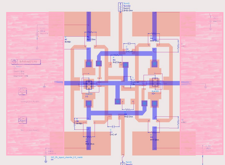
I am rahul vishwakarma i have bought this IC 4303 for the application of Negative impedance converter.The simulation part is done and i am getting result. The problem arises when i have fabricated the structure and measuring the result but the desired result is not coming.

1. I have checked the IC in Khz range (by making voltage follower circuit) and is seems ic was giving desired response.My doubt is how i can check ic in GHz range (my desired freq range is 2 to 3.5 GHz)?

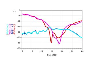
2. The output which i am getting (by applying 6 to 9 volt dc in +-VDC) S21 is around -20db which is not desired it should come in between 3db to -7db. Seems like the Opamp IC is not turning ON. Can you suggest me what should be taken care to turn on IC in GHz range.

3. Power down pin of IC i have connected to +VDC supply(ranging from 1.1-2.5 volt) (as suggested in datasheet to turn on IC min 1.1 volt should be given).

4.The desired result of NIC ckt has came in schematic Simulation and cosimulation (ckt+ layput)  design is achieved. But while measuring practically it is not coming.I have doubts weather IC is turning on or not as s21is around -20db.

looking forward to hear from your side as soon as possible

Thank you

Rahul

  • Hi Rahul,

    In order to best resolve the issues you are seeing in your application; would you mind sending your schematic and simulation file. I did notice you mentioned the expected frequency range of 2 GHz - 3.5 GHz. The THS4303 is designed to work at 1.8GHz, therefore frequencies in the range given might be too high for the device. You also mentioned your concern of the device maybe not being properly powered on. The 1.1V power-on voltage threshold the characteristics table lists are relative to the supply voltage the device is being powered with. May I ask what voltage supplies are being used as well as the input signal characteristics? This information will help narrow down a possible cause for these issues.  

    Best Regards,

    Ignacio

  • 1.the schematic diagram and its result is attached

    The s parameter response is for Co-simulation case which is my desired result

    2. As you said ths4303 works at 1.8 Ghz but in the data sheet it is written its typical value of gain at 1.8 GHz but the small signal gain is more than 10 db upto 4GHz. as shown in above graph.So I am utilizing the gain value upto 3.5 ghz

    3.The DC supply i am applying varies from 6 to 9 volt. and two port are connected to vna to measure s parameter as shown below

    top and bottom view is shown above green wire is +vdc and  brown is -vdc.

    The measured response of fabricated prototype is shown below

    s44=s22 s33=s11, s43=s21, s34=s12. which is not matching with simulation result

  • Hi Rahul,

    I don't see any components values in the schematic.

    And you don't have a ground plane on your printed circuit board. How are you connecting the signal grounds? By wires? I strongly recommend to follow the example layout given in figure 52 of datasheet. You urgently need a ground plane.

    Kai

  • hi kai,

    1. one the pcb the ac ground and dc ground is separated. I am attaching indicated image of ac and dc ground.

    The SMA connector is having ac defected ground and a center dc ground line is running  on the back side as indicated in above figure. will it be sufficient to have ground in the PCB . The application I am looking  to use this NIC  I cannot use full ground plane.

    The wire is used to provide dc supply to PCB.

  • Hi Rahul,

    I'm sorry, but this will not work with a 1.8GHz OPAmp. The wires will entirely ruin the performance. You urgently need a solid ground plane as shown in the datasheet.

    Kai

  • Hi Rahul, 

    Like Kai mentioned I do believe the layout is a concern for such a high frequency part. Another concern is the supply voltage being used. The device's datasheet recommends 5V in a single (+-2.5 in a dual) supply configuration for optimal performance and an absolute max of 6V. Anything beyond this value can cause serious damage to the device.

    Best Regards,

    Ignacio

  • hi Kai and Ignacio,

    1.This  circuit in MHz with the same circuit configuration which worked with the same ground configuration.The circuit worked for that case.the fabricated prototype gave result same as that of simulated.

    2.The power supply to the IC reaching max is 2.5 volt when i am giving 9 volt then through limiting resistor the voltage at the IC input is 2.4 volt. so the IC is not getting damaged.

    3.please tell me this ic will work at only 1.8GHz there is no significance of datasheet small signal gain vs frequency for the frequency range of 1 To 4 GHz.where the gain is more than 10 db(19-10 db)

  • Hi Rahul,

    I cannot say anything about your circuit when I do not see the component values in the schematic.

    That this circuit works at 1MHz does not mean that it also works at 1.4GHz. 1.4GHz is a 1400 times higher frequency!

    You could easily improve the ground routing of your board by adding a ground plane and ground fills like hinted below:

    If you want to make the circuit work at 1.4GHz then banish all the wires. Every single cm of wire adds 10nH inductance which means an impedance of 88 Ohm at 1.4GHz. A 30cm long cable introduces an inductance of 300nH into the signal path which gives an impedance of 2640 Ohm at 1.4GHz. No 1.4GHz circuit which I know will tolerate so long wires.

    You may separate AC and DC ground for any reason which I don't know, but at HF there should be a low impedant connection between them. And this on your board. Only by this you can avoid the long wiring.

    Please give the component values of your circuit and explain why you want to separate AC and DC ground.

    Kai

  • Hi Kai,

    2. There is no particular reason for separating AC and DC ground.

    " You may separate AC and DC ground for any reason which I don't know, but at HF there should be a low impedance connection between them." Them means AC and DC ground?

  • Hi Rahul,

    I would strongly recommend to carry out a TINA-TI simulation of your circuit and a phase stability analysis as shown in this thread:

    https://e2e.ti.com/support/amplifiers-group/amplifiers/f/amplifiers-forum/963567/stability-analysis-and-open-loop-gain-measurement-of-op-amp-in-nic-circuit

    Run the simulation of your circuit with an ideal OPAmp and with the THS4303, to see whether the THS4303 is able to do what you want.

    Kai