This thread has been locked.

If you have a related question, please click the "Ask a related question" button in the top right corner. The newly created question will be automatically linked to this question.

OPA828: Survey of transimpedance compensation solutions - where did this one solution come from?

Part Number: OPA828
Other Parts Discussed in Thread: OPA3S328

So I had gotten involved in what is out there in compensating a transimpedance design, There is a newer one I will mention at the end that seems very accurate, wondering what equation sits behind that - but first

This app note repeats a very common (ancient) approach but then reports a BW that is quite incorrect, https://www.ti.com/lit/an/sboa354/sboa354.pdf

Here, the OPA828 (45MHz GBP) is used with a 100pF detector and 50kohm gain to target about a 1.1MHz small signal BW. 

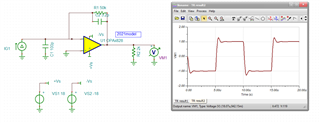
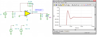
Here I stepped through some testing - this app note uses the old idea of putting the feedback pole at the Fo frequency, that will in fact give you a close loop Q of 1 extending the BW and peaking about 1.25dB. Not really very desireable step response and easy to fix. 

OPA828 model tests and Zt testing from SBOA354 document TI only.docx

The improved Cf solution we have been using in high speed TI amps for many years is in here, 

4784.Transimpedance design flow using high speed op amps.pptx

The ADI photodiode design wizards seems to be doing this correctly,following what I had in the earlier articles I wrote on this topic. 

https://www.edn.com/control-frequency-response-and-noise-in-broadband-photodetector-transimpedance-amplifier/


A more recent tool was developed by Hasan and placed into this e2e - it seems to match what I was doing, but is it perhaps doing some else like Jerry Graemes slightly more accurate equation in the word file here? 

I would suggest you make the excel tool in this link more findable and either get rid of or fix the misleading info in SBOA354

https://e2e.ti.com/support/amplifiers-group/amplifiers/f/amplifiers-forum/956151/faq-transimpedance-amplifier-calculator?tisearch=e2e-sitesearch&keymatch=faq%3Atrue

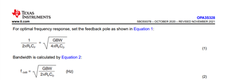
  • And along these same lines, I was looking at this relatively new switched gain device the OPA3s328, these equations are correct where that one for Cf has that 4 in the denominator instead of 2. The extra 2 in the square root is essentially setting the target Q to 0.707 or butterworth as per the High speed design flow, So it is correct in some places it seems, 

  • Michael,

    You are correct that the BW of the first app note is not precise.  But this is because the main point of the app note was to show that the OPA828 design circuit meets / exceeds the TIA bandwidth requirement 1-MHz while being stable. Obviously, you can then tweak the feedback capacitor to increase phase margin  - the suggested circuit has much more than 45-degrees of phase margin so it is quite stable - modify Q, or reduce bandwidth as needed. The app note simply suggest that the OPA828 unity gain bandwidth (fGBW) is more than sufficient to support the TIA design requirement. 

  • Not sure that I would be ok with the step response produced by the app note Cf. Still wondering where Hasan tool equation came from? or what it is. 

  • Hi Michael,

    Not sure about the Hasan tool.  I'll transfer this to the high speed forum to address that.

    Regards,
    Mike

  • You guys say that occasionally, as far as I know there is no seperate forum, just different people. 

  • Yes it's all internal on our side.  FYI there are several people out due to the holiday week so they may not get back to you until next week.

    Regards,
    Mike

  • Michael,

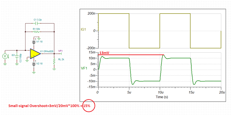
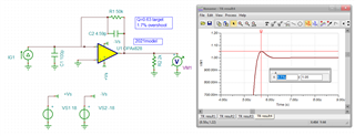
    Just so you don't have to wait until next week, I would say that your step response above uses a large-signal instead of small-signal and therefore it does not say much about the circuit stability (Hasan used 100mV step).  If you run the same transient analysis with a small-signal input, it shows a very stable circuit with overshoot of just 15% - far less than maximum recommended of 25% (see below).  I'll let Hasan answer your other questions.

    OPA828 TIA stability.TSC

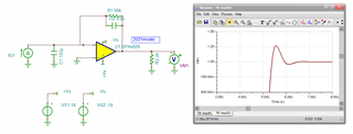
  • So the 2V step I had been doing is also right around 12.5% overshoot, about the same as the small signal

    An ideal Q=1 step should be about 16% overshoot, which is another part of Hasan's spreadsheet

  • And just out of curiosity, that Maxim solution for Cf (2.88pF in the attached word file) is a little more accurate to set the pole at the intersection of the noise gain and GBP, here it hits 17% overshoot more inline with the theoretical 16.3% for a Q of 1, 

  • And one more example, I often will target 0.63 =Q for good step response - setting the feedback pole at 0.63*1.1MHz requires a 4.59pF feedback C and gives about 2.5% overshoot, little more than Ideal but I have not verified the model input C yet - needs to be 15pF total Cdiff+Ccm for the analysis to match desired. 

  • So to close this out, 

    the earliest discussions I can find simply set the feedback pole at Fo and yield a 45deg phase margin and lots of ringing. (Walt Jung's comprehensive Op Amp Applications Handbook, page 273). This primitive approach (which I am sure showed up much earlier in his work) has been copied over ad nauseum to the detriment of many designs. 

    The later developments that I did approximate a solution for Cf that uses Q=P1/Fo where P1 is the feedback pole - the high speed group has been using that flow since about 2001. 

    That is what is in Hasan's tool (from Samir's articles he adapted from my earlier work). Graeme's later book gives a more detailed equation (page 58) for Cf including zeta that seems to match what Hasan's tool delivers.

    I still think the tool Hasan did shoule be made easier to find, closest thing I know of from TI that approaches the ADI photodiode design wizard.