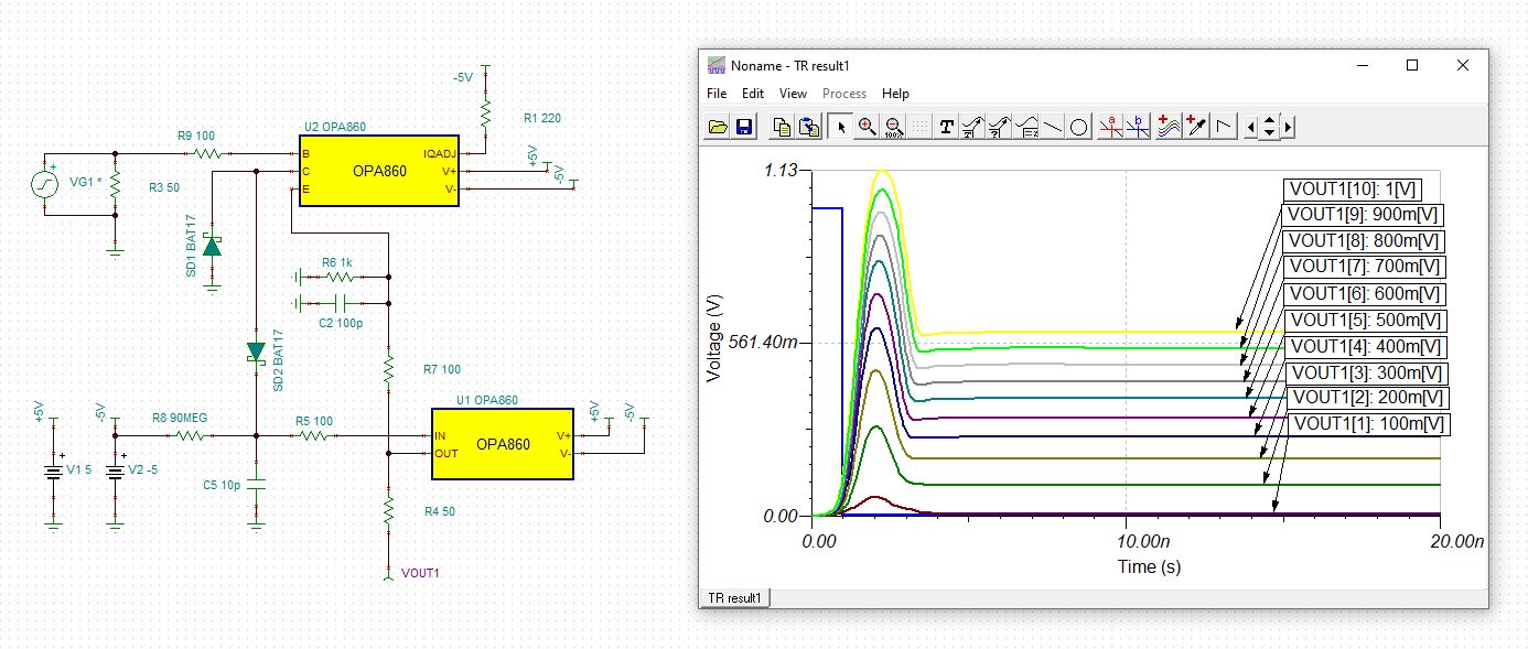
This thread has been locked.

If you have a related question, please click the "Ask a related question" button in the top right corner. The newly created question will be automatically linked to this question.

OPA860: peak detection circuit

Part Number: OPA860

Hi team,

One of our customer's issues, could you please provide some troubleshooting suggestions

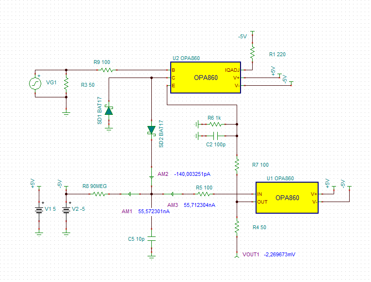
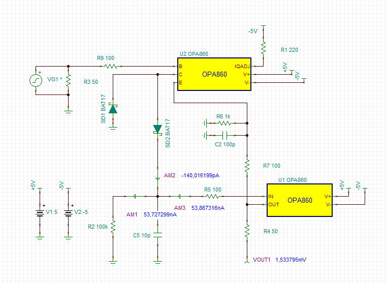
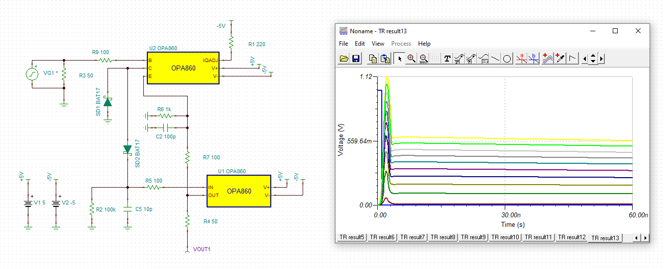
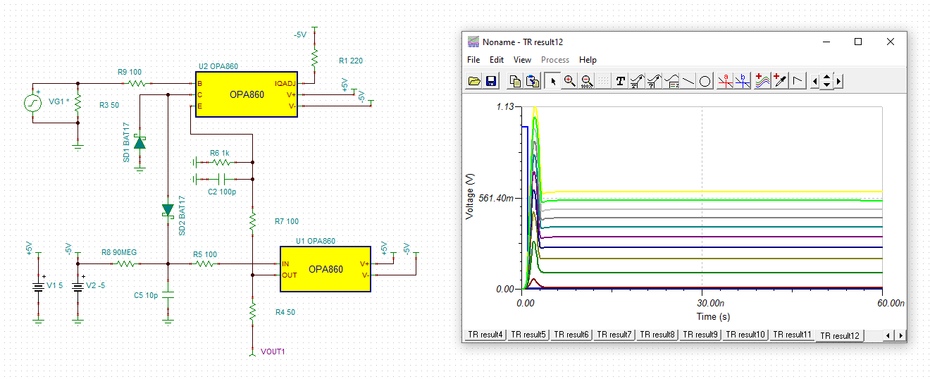
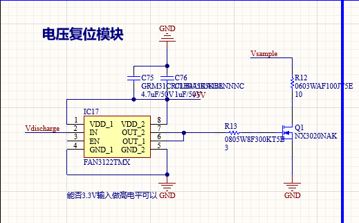
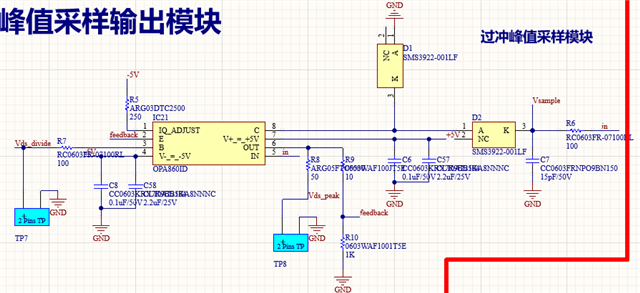
The customer made a circuit board based on the circuit in the post below (from Kai) and after testing found that the output was around 3.8V regardless of the input signal. Could you help analyze the cause of the problem?

The diode part number used in the figure is SMS3922-001LF.

https://e2e.ti.com/support/amplifiers-group/amplifiers/f/amplifiers-forum/1004949/peak-detection-circuit/3723066?tisearch=e2e-sitesearch&keymatch=PA860%3A%20peak%20sampling%20circuit%20of%20OPA860#3723066

Best Regards,

Amy Luo

  • Hi Amy,

    this can happen when the leakage current of the Schottky diode SD2 is so small that it cannot fully absorb the input bias current of the buffer of OPA860. In this case you need an input bias current cancelation scheme, for instance provided by R8:

    anny_peak_1.TSC

    Because the input bias current of OPA860 can widely vary, you may need to adjust V2 and/or R8.

    An alternative to the input bias current cancelation is to mount a bleeding resistor in parallel to C5:

    But this will unwantedly speed up the decay time:

    I know, all this sounds rather uncomfortable. But hey, this circuit can peak detect 1ns signals...

    Kai

  • Hi Kai,

    Thank you very much for your response.

    When the customer connects the circuit according to your recommendations, peak detection is actually possible and is maintained well. But this circuit doesn't seem to have that strong detection capability for narrow pulses. When the peak he tested was around 2V, the circuit takes about dozens of ns to reach its peak. I don't know if there is any way to make it detect the peak of a narrower pulse

    Best Regards,

    Amy Luo

  • Hi Amy,

    hhm, dozens of ns? Then there must be something wrong with the circuit. The OPA860 may have lost its operation point or is hanging in saturation. Or has the customer connected a discharging device to the sampling cap? Only a GaAs-MESFET would do here, if at all.

    The circuit is very sensitive to the layout. HF methods must be used, like using a solid ground plane, etc.

    Yes, the circuit is at the border of what is possible with the OPA860. This circuit works with a decompensation network provided by R6, R7 and C2. It may be helpful to experiment with these component values. And it may be helpful to experiment with the sampling capacitor C5.

    For many reasons these circuits only work properly in a rather limited input signal range. An amplitude of 2V may be too high for this circuit because the OPA860 shows a limited slew rate. I would try an input voltage divider to decrease the input voltage and by this the slew rate. And if a large range of amplitudes has to be handled, then using several circuits in parallel each with a suited input voltage divider to cover the whole range could be helpful.

    The Schottky diodes play a major role here. They should be chosen for ultra low transition time and junction capacitance. So, experimenting with different diodes may also help.

    Kai

  • Hi Kai,

    I'm the person who ask the question.You are amazing, and after I removed the discharge device shown in Figure 1 from the sampling capacitor, the circuit's ability to sample ns-level signals was greatly improved, and I was able to easily complete my work requirements. And what I want to ask is that If I want to drain the charge on the sampling capacitor at a desired moment, where should the discharge device be connected to the circuit shown in Figure 2? Thank you very much!

    Figure 1  discharge device

    Figure 2  peak detector circuit

  • Hi,

    some years ago I built the above circuit with the OPA660. To discharge the sampling capacitor (here 33pF) I used this scheme:

    I used a GaAs-MESFET because it offers an ultra low charge injection. If the discharging transistor is not providing a very small charge injection, on the other hand, you will unwantedly charge the sampling capacitor by a portion of the "Reset" signal. This would mean that you cannot fully discharge the sampling capacitor. 

    Another option is to discharge the sampling capacitor by the help of a high ohmic resistor which is all the time in parallel to the sampling capacitor and need not to be switched.

    Kai