This thread has been locked.

If you have a related question, please click the "Ask a related question" button in the top right corner. The newly created question will be automatically linked to this question.

THS4541: OPA657 + THS4541 circuit review and OPAmp for negative rail

Part Number: THS4541
Other Parts Discussed in Thread: ADC3683, , OPA657, OPA365, THS4551, ADC3683EVM, LM7705, LM27761

Hi,

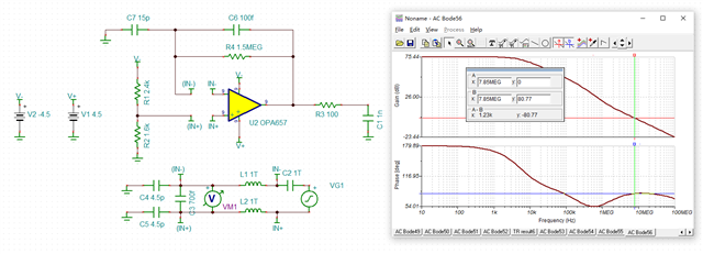
I'm designing a four channel optical detection front-end with OPA657 and THS4541.(connected to following ADC3683)

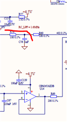
Main Circuit are shown below. 

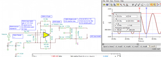
I used OPA365 to generate a -0.6V to maximize the output swing range of the THS4541. I'm not sure if it's a correct way to do so, considering stability and noise.

It would be very appreciated if anyone can take a review, thanks !

  • Morning Follin, 

    Couple of things, 

    Your interstage RC filter looks to be about 1.6MHz. Kind of low for a part as fast as the THS4541, you may be able to drop down to the THS4551 and save power. 


    Not sure you really need that extra -0.6V reference, the FDA will act to level shift the output swing around the CM voltage even with negative input signals - normally you would just ground the path on the other side and with that interstage filter, you would normally match that network to get better CM suppression on a fast step. 

    Really cannot start TINA sims without the detector capacitance, the 1st step is always stability check in the Zt stage. Can you provide that. 

  • Hi Michael,

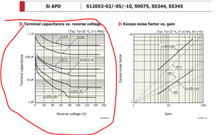
    the APD seems to be this one:

    s12053-02_etc_kapd1001e.pdf

    Kai

  • Thanks Kai, Happy new year to you and all the folks on this forum

    And we are still left with the reverse bias question, 

  • A Happy New Year to you too, Michael Relaxed

  • Hi Michael,

    Thanks for your reply and Happy new year to you Slight smile

    - THS4541 vs THS4551

    I used THS4551 in last version but was told that it's better to use THS4541 amplifier meantioned on the ADC3683EVM.

    (https://e2e.ti.com/support/data-converters-group/data-converters/f/data-converters-forum/1159805/adc3683-glitch-and-input-of-adc)

    I'm not sure if there's some specical reason behind but I'd like to change back to THS4551.

    - -0.6V rail

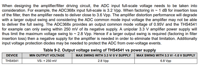
    In the datasheet of ADC3683 it shows the negtive rail is required to maximize the swing range due to the 250mV headroom of THS4541/4551.

    And in the 3683EVM LM7705 is used to supply -0.23V as the negtive rail.

    I think I can do the same as the EVM design, I'll put on a LM7705 set to -0.23V around and also keep a 0ohm resistor to ground.

    The LM7705 seems to have very large noise (10mV? in the datasheet), and target is to make the noise under 200uVpp, then I find LM27761 but the output is -1.5V to -5.0V. 

    So shall I use LM7705 or keep the opamp follower design? 

    - APD 

    The range of the reverse bias voltage would be around 80-160V.

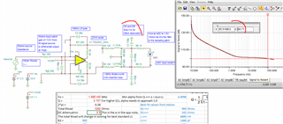
    And I used 15pF for simulation:

    It seems it's stable. (And the 0.1pF capcitor is only the capacitor welded, there's still some parasitic capacitor of the 0805 gain resistor and PCB trace.)

    And would you mind expaining " with that interstage filter, you would normally match that network to get better CM suppression on a fast step. " a bit more?

    Looking forward to your reply and thanks again!

  • Hi Kai, thanks for posting the datasheet and happy new year to you!

  • Hi Follin,

    a Happy New Year to you, too Relaxed

    The LM7705 seems to have very large noise (10mV? in the datasheet), and target is to make the noise under 200uVpp, then I find LM27761 but the output is -1.5V to -5.0V. 

    The LM7705 is a charge pump and like any other charge pump it generates a certain ripple voltage at the output. To be honest the ripple of LM7705 is very low compared to other charge pumps. With reason the datasheet calls the LM7705 a "low noise negative bias generator".

    Also, the noise can be heavily decreased by using low pass filtering at the output of LM7705. See this appnote:

    3157.sbaa373.pdf

    And then there's the huge "power supply rejection ratio" (PSRR) of THS4541 which furtherly suppresses the output voltage ripple of LM7705 by about 100dB. 4mVpp / 100000 = 40nVpp which is way below your 200µVpp goal.

    Kai

  • Morning Folin, 

    If you read the discussion for the converter EVM using the THS4541 it says they see the same glitch as you do - I think this is because they did the filter wrong, normally you want the diff C right at the ADC inputs as the last element, you inductor being last is why the glitch is so large. 

    THS4541 was probably used there on the ADC EVM due to its better HD to higher F. If you do not need that higher F, the THS4551 might be good enough. 

    Also, that discussion of getting more swing out of the THS4551 with a negative supply - so the ADC is needing 3.6Vpp max, or 3.8Vpp at FDA output if it is a -1dB insertion loss filter. Each output pin of the FDA needs to swing +/-0.95V to do that. On 3.3V supply that is pretty easy without any special effort. 

    Looking at the ADC input spec, 3.2Vpp is full scale, normally you target -1dB from that for operation, so if the filter also had -1dB, you need 3.2Vpp at the FDA output or +/-0.9V on each FDA output pin. The CM is pretty constrained, but 1V is allowed. Then, if you implement the filter with a DC CM attenution (by grounding w final R's, we can operate the FDA with CM say at 1.1V and hit 1V at the ADC, That 1.1V output CM with +/-0.9V swing should be fine on 0 and 3.3V supplies. 

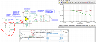
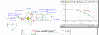
    here is the beginning of  redesign, 2nd order RLC at 1.8MHz with 10MHz feedback, that little spike is phase margin issues with the feedback cap, I usually fix that with a diff cap across the input pins, 

    yes, there we go, diff input 100pF and 20ohm inside the output pin loop will de-Q that, 

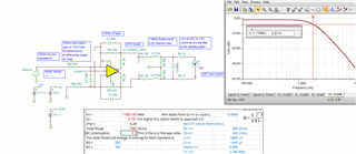
    Now just looking at the filter to the ADC, about 1.77MHz, 

    And then just looking at one side sine wave at 100kHz, looks about right, 

    And this file, more to do here, but this should give you some ideas, 

    FDA_THS4551 2019 model with postfilter to ADC3683.TSC

  • here I made an obvious adjustment to split the final C into CM and DM parts (some folks think this is a good idea for glitch suppression), same filter shape and here is the SNR using 1.02Vrms reference (0.9*3.2Vpp max). about 100dB just in this stage, 

    And the modified file, 

    4150.FDA_THS4551 2019 model with postfilter to ADC3683.TSC

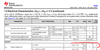
  • And just to be super clear, this comment is a hard mistake - apparently they forgot this was an FDA with two outputa swinging 180deg out of phase,So correcting their math and granting 0.25V to each supply on 3.3V the max is 2*2.8 or 5.4Vpp, plenty for this app. Of course trying to meet the ADC input Vcm at 1V will actually set the max. 

    The 0.25V min output headroom is also very convervative I think, it is more like 0.2V on the THS4551 and is a tested spec (Aol test I think), 

  • Hi Michael, 

    Thanks for your considerate guidance,it's much more clear to me now.

    And is my stability simulation of the OPA657 part right? 

    By the way, I've gone through the TI-lab lessons and related articles, but haven't found useful content with respect to the design from FDA to ADC, especially the anti-glitch and filter part - For instance, why the LP pole of the FDA is set at 10MHz in your design?

    Do you know if there're any articles/books that can help me on this?

  • I guess in the datasheet since the negtive rail headroom is 0.25V and VCM is supposed to be 0.95V, so the maximum swing range is calculated to be (0.95-0.25)*2*2 = 2.8Vpp. 

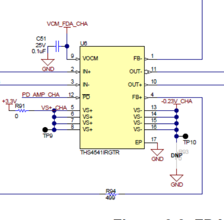
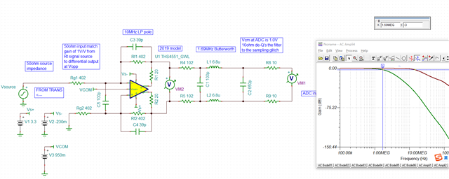
  • And for some reason I cannot change the VCM and the layout around the filter part in this version, so currently the design would be:

  • yes, that looks real good - and the -0.23V supply should provide the needed output headroom, 

    I sometimes just pick a target F-3dB assuming there is an unstated flatness concern, if 1.69Mhz is what you want, so be it. You do not have any insertion loss now in the filter, keep in most ADC's spec a -1dBFs for max input, so that would be .9*3.2Vpp, or about 2.9Vpp or 2.9/4 = .725V down from 0.95Vcm giving 0.225V min. in theory, that would be ok on the THS4551 with a ground on the negative supply looking at the datasheet. 

    yea that whole glitch thing is murky - the ADC char guys just try things mainly with only balun inputs. I had several of them strongly suggest small caps to ground at the inputs since the glitch is common mode. 

    Also, this sampling input will often pull a clock rate dependent CM current - don't see that uA/MHz spec line in this part but I was able (finally) to get that into the more recent high speed ADC's. That causes a CM level shift witht the series R in the filter. Just a possible concern the ADC guys should address, 

    I think I remember the early disscussion on this ADC where they wanted a better driver. Back in 2017 I was piecing that proposal together doing an even lower distortion and noise verions of the THS4541. I suppose that effort faded away when I left. Those are very difficult business plans to sell as the volumes are so low if tied to just these ADC channel counts. 

    Did a lot of bench work on these very high performance ADC input filters in this document where I implemented a direct measurement of what was happening at the ADC input pins. This one was delivering better than -115dBc through 100Mhz at very low power to the ADC inputs, but only AC coupled requirements. 

    ISLA214P50_ISL55210 EVM board documentation.pdf

  • Thank you, Michael, really appreciated. And I find that for we users it's always very hard to understand the design clearly but rely on the simulation and tests :(