This thread has been locked.

If you have a related question, please click the "Ask a related question" button in the top right corner. The newly created question will be automatically linked to this question.

THS4541: Review of THS4541 Outputs for High votlage swings

Part Number: THS4541
Other Parts Discussed in Thread: ADC3669, , LMH5401, TINA-TI

Hi,

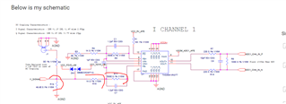
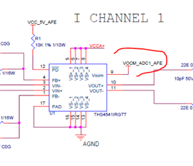
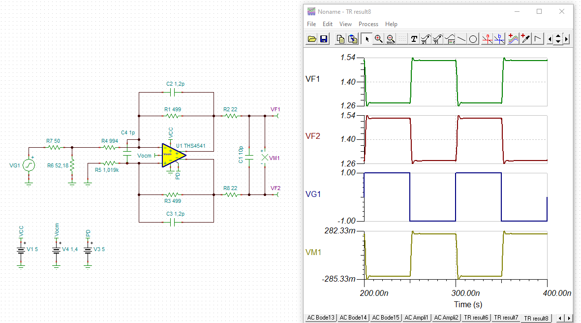
Below is my schematic

Vocm is open and not connected below are my observed outputs

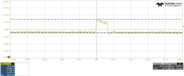
Q1 : as per datasheet VCM will be mid supply but why my output is at 2V ?

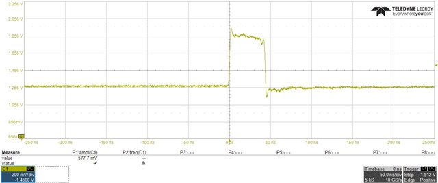
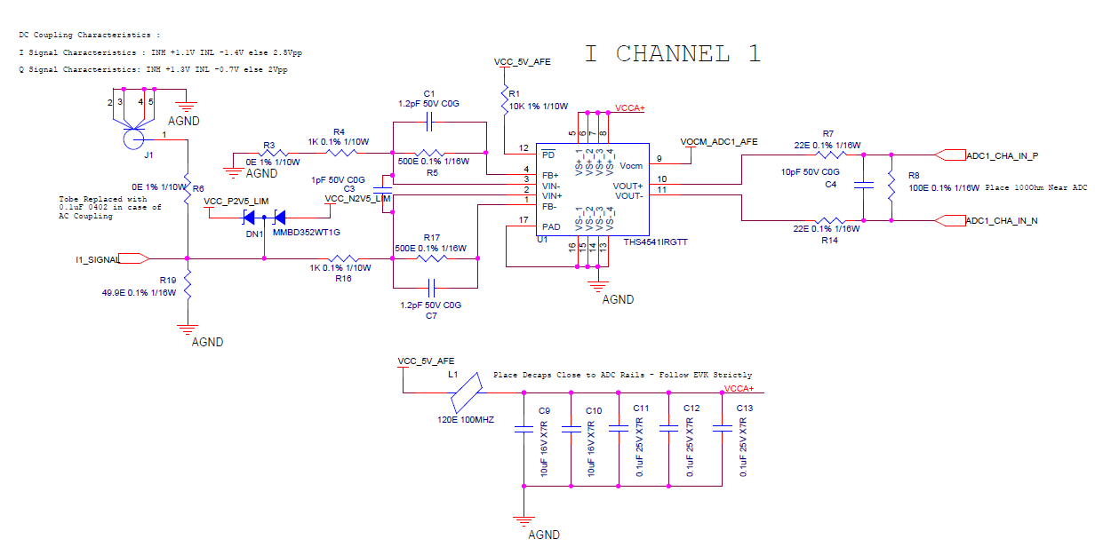
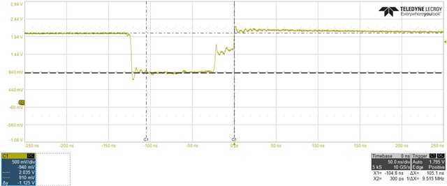
i have incorporated a voltage limited to protect my adc from high voltage inputs, so when a 3v3 input is given the diodes are supposed to supress the voltage or limit the voltage to 2.5, but its not the case, the output is as below

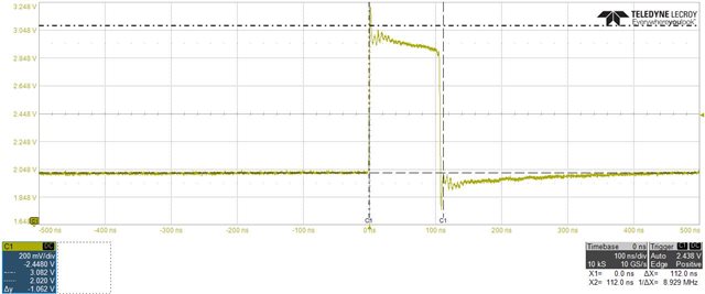
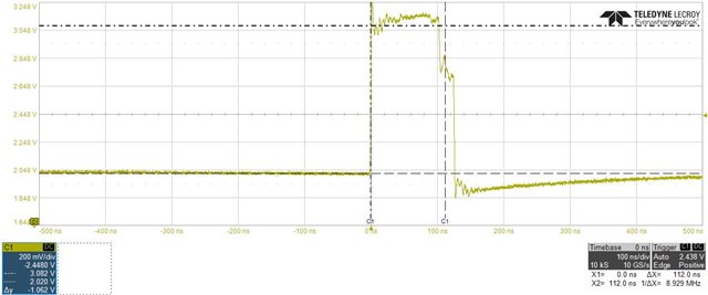
even if i increase the input voltage much furter , the limiting happens only up to 3V, but not 2.5V

the behavior is little different for negative input voltage 

the output for a negative input voltage of -3v3 is as below and i assume ADC can bear this

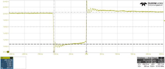
below is output for input voltage of -4.5V 

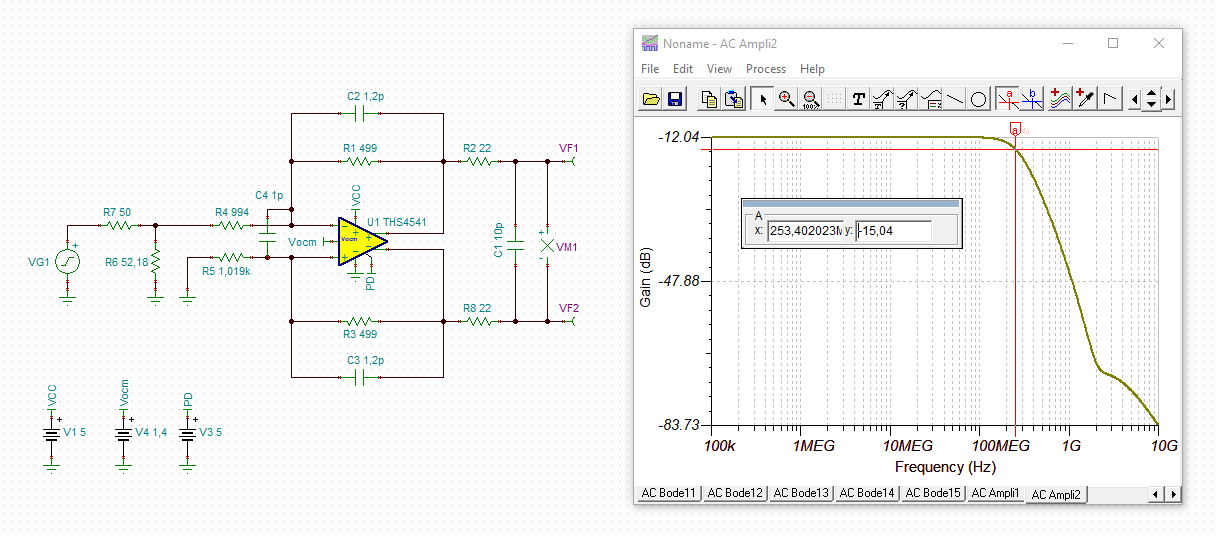
i am quite confused on this behaviour kindly comment on how to restrict voltage, so that i can protect the ADC from spurious inputs which may exceed limits.

The ADC info can be shared over mail, because the TI ADC3669 is not yet released in market.

  • hey Shyam, 

    Without going through everything, I am guessing you a little off on your R setups, I am guessing you are coming from 50ohm source and want a 50ohm termination at a gain of 0.5. 

    You are not getting that right now due to the active input impedance of the single to diff FDA setup, 

    If you want to get that here are the correct R values, exact here, get close

    Rf on both sides 499ohm

    Rt to ground on input side 52.18ohm

    Rg1 on signal input side, 994ohm

    Rg2 on the other side to ground, 1019ohm. 

    Might not make much difference to your question, but might as well get this right - i put this discussion in the datasheet under single to diff resistor setups where you will see a quadratic solution for Rt, the termination resistor. 

  • Thanks for your valuable response,

    The scheme is already reviewed from one of the TI engineers offline, i am ok with the gain settings

    but i am not satified with voltage not being limited by diodes when the signal is positive, are the opamp characteristics playing a role in not limiting the outptu voltage same for both +ve and -ve inputs ?

    also the output vcm is supposed to be midsupply as per datasheet, but its 2v why ?

  • We can only work with what we see here, not hidden discussions, that might be approximately correct. 

    What is Vocm from the ADC? and are you coming from a 50ohm source, 

  • 1. Vocm from ADC is 1.4V as per datasheet, in my hardware i did not mount ADC yet 

    so up on applying 1.4v externally from supply, i have seen the signal to show commond mode voltage of 1V exactly

    2. yes the source is a 50ohm source

  • Hi Shyam,

    there are several issues:

    1. The protection diodes cannot clamp the input voltage to 2.5V. This would mean that the forward voltage drop across your diode would be zero Volt. But this is not the case. According to the datasheet of MMBD352 the voltage drop is about 0.42V at a current of 1mA. So, when flowing 1mA through the protection diode the input voltage will be clamped to 2.5V + 0.42V = 2.92V which is what the scope plot shows.

    2. There's no current limiting in front of the protection diode at all. No current limitings means that the protection diodes can easily be destroyed when the source voltage becomes higher then 3.0V.

    3. The current through the protection diodes can make issues in your circuit, because this current must be absorbed by the 2.5V voltage regulator. If the voltage regulator is not able to absorb this reverse current, the regulated voltage may rise and the regulator may even be damaged.

    4. To protect the ADC input you will need to mount the protection scheme betwen the output of THS4541 and the input of ADC. With your scheme the ADC input may still be in danger during power-up and power-down.

    Kai

  • This approach of protection is directly taken from TI reference design, the same problem would be existing there also, 

    50-Ohm 2GHz Oscilloscope Front-end Reference Design (ti.com)

    i am using a 0.5gain infront of ADC to limit these high voltages

    Can you suggest any reference design to go ahead in protecting ADC ?

  • Hi Shyam,

    yes, but figure 2 is saying that the input has to be driven by a 50R source which will provide a certain current limiting.

    Also, the reference design shows a different circuit with a different OPAmp. During the risky power-down of circuit the relays of pi-attenuator completely disconnect the OPAmp from the input signal. And the used LMH5401 withstands higher input voltages than the THS4541.

    I would protect the input of ADC3669 as shown here, by the help of resistive voltage dividing and resistive current limiting:

    DC104_ADC3660_REVE_Sch.PDF

    Kai

  • I have removed the input 50Ohm resistor, which made the output vcm to shift to 1.25 but not 1.4V, are the Rt, Rf, Rg are to blame for this ?

  • Hello Shyam,

       Did the calculated resistor change fix the issue?

    Thank you,
    Sima 

  • You mean to say the suggested changes of 

    Rf on both sides 499ohm

    Rt to ground on input side 52.18ohm

    Rg1 on signal input side, 994ohm

    Rg2 on the other side to ground, 1019ohm. ?

    are you sure this might be the issue, i need to get these odd values ordered.

  • Hello Shyam,

       Yes, correct. 

       Using Kai's Tina-TI file, here is the transient simulations based on the original resistor values:

       The difference is noticeable in the output differential voltage. There is an balancing issue which will affect the output common-mode differential. Is this around the same differential you are seeing on the board?

    8461.shyam_ths4541.TSC

    Thank you,
    Sima