This thread has been locked.

If you have a related question, please click the "Ask a related question" button in the top right corner. The newly created question will be automatically linked to this question.

OPA2625: How to improve SNR, HD2 and HD3 of an 18-bit SAR ADC when OPA2625 is being used to drive the differential inputs of ADC?

Part Number: OPA2625
Other Parts Discussed in Thread: OPA838, THS4561, THS4551, THP210, THS4541, ADC3683

Hi,

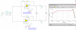
We have built an EVM for an 18-bit, 65MSPS SAR ADC for which we are using ADT1-6T+ transformer and OPA2625 in the below circuit configuration to drive the differential inputs of the ADC.  

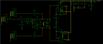
The theoretical noise floor (SNR) of ADC is around -85 dBFs. We expect the input drive circuit to have a much better noise performance so that it does not limit the noise floor of the overall system. It must also have good distortion performance (HD2 and HD3 is what we are mainly looking at). The ADC input must be at 3.2V peak-to-peak. Based on these constraints, OPA2625 was chosen considering the noise, HD2 and HD3 values specified in the datasheet. The op-amp is being operated in the high-drive mode.

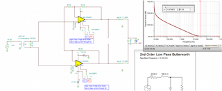
In the above circuit, the feedback resistors R102 and R103 are set to 3K ohms and resistors R101, R104 are set to 1K ohms to obtain a gain of 4. The setup is being tested at an input frequency of 200KHz and ADC sampling frequency ranging from 22MSPS to 50MSPS. Here are many other configurations we have tried:

-Vary the gain (We would prefer to keep it larger so as to avoid having to supply a large RF input amplitude. Also, we are seeing a poorer performance when the inputs to the opamp need to swing high so as to compensate for lower gain)

-Keep the gain constant, but change the absolute values of resistors from low to high values

- Varied the supply rail values (Contrary to what is mentioned in the datasheet, we are obtaining better performance at a supply of Vs+ = 3V and Vs- = 0V)

- Added a lowpass RC filter (R = 5ohms and C = 200pF to ground) at the outputs of op-amp so as to limit the noise bandwidth

- Added a capacitor of 60pF in parallel to the feedback resistor (constraining that gain of the amplifier has to roll-off before the cutoff frequency of the RC filter) so that loading on the amplifier output can be minimized. Our idea was that quicker the capacitor starts to dominate the feedback as compared to the 4K ohm resistor, sooner its contribution to thermal noise at the output disappears.

Unfortunately, none of the above cases have yielded fruitful results. The SNR doesn't go beyond -72dBFs, HD2 and HD3 are around -75dBc in the best case. What's worse is that completely removing the op-amp and driving the ADC input with only the transformer improves our results to an SNR of -77dBFs, HD2 of -105dBc and HD3 of -90dbC. But, eventually having a transformer in the input path is not feasible as we are looking to provide DC sampling ability as well.

Please suggest any changes in our circuit that we may try to achieve better performance than what we are seeing now. Changing the op-amp could also be considered, in which case, please suggest a suitable one (I did come across articles that suggested current feedback op-amps as better ADC drivers than voltage feedback ones. If so, kindly elaborate the reasoning as well.)

  • Couple of quick things Akash,

    1. Where is your DC bias current path for the V+ inputs to the op amps?

    2. This differential I/O op amp circuit sometimes has a common mode oscillation - probably not here, but we did see that in the OPA838 decomp device - I put a discussion of that in the data sheet, 

    3. You will need to provide some type of filtering between the op amp outputs and the ADC inputs or you will get the broadband noise of the op amps into the ADC, i usually use an RLC filter - low insertion loss design, you probably have something there, but would need that for full analysis

    Your question (ADC spec degradation) is fundamental, and we spent a lot of time on that back in the early 2000's - here is slide deck reporting those results, 

    Normally, I would have used an FDA for this interface, depending on frequency range look at the THP210, THS4561, THS4551, THS4541. And normally, the balun needs a matching R on the secondary - I have done a great deal of work (and articles) on that topic if you need help there. 

    HSP_ADCinterfaceOct2006.ppt

    Techniques to improve Distortion at Freq Less than 1MHz.ppt

  • Hi Akash,

    what ADC are you using?

    I ask because the manufacturer of ADC usually recommends a perfectly matching ADC driver for his ADC.

    Kai

  • Hi Michael,

    1. R2 and R3 jumpers are replaced with 250 ohms. That should enable the DC common mode voltage to reach the V+ input pins and provide a path for bias current flow. Is this what you meant?

    2. I shall look at the discussion, but yes, I have checked that our common mode does not seem to be oscillating.

    3. We have a lowpass RC filter as I have mentioned above. R = 5 ohms serially in P and M path, and a 100pF capacitor differentially between P and M outputs to limit the noise bandwidth. We have also tried separately with an RL filter (R = 50 ohms parallel with L=40nH) each on P and M path so that propagation of any non-linear glitch towards the input due to sampling operation of the ADC can be prevented.

    Thank you for the slide deck, they have been quite insightful. I can broadly understand that one ppt recommends that a balun performing the single-ended to differential conversion followed by a FDA would have good results and the other ppt illustrates the possible advantage of a current feedback amp over voltage feedback one. While I don't know about the feasibility of changing the amp at this stage, I will try adding the class A current to OPA2625 to see if performance can be improved.

    We have also tested with a wide range of drive circuits. We are currently using THS4541 alone as part of the drive circuit with input resistance at 200 ohm, feedback resistance at 800 ohm and the same RC filter as before. There is an improvement in HD2 and HD3 as compared to OPA2625, both are at around -90dBc. Yet the SNR is only around -77dBFs. We did have a 50 ohm matching resistance at the secondary of the transformer, and since it is a 1:1 transformer, we transformed the impedance to the primary side so as to avoid loading the transformer. (To prevent possible distortion due to core saturation at higher secondary currents). As I said, we have found just the ADT1-6T+ balun alone to be giving the best performance, but we want DC coupling option as well. Any further insights you can provide will be very useful.

  • It is an improved version of ADC3683 from which we hope to get better linearity. Since TI is the manufacturer in both cases, it is upto us to suggest the best ADC driver. Our current driver circuits closely resemble the ones suggested for ADC3683

  • Very difficult to make any headway with so many variables without a sim working, here is a start, I have the supplies at +/-2.5V and V+ biased ground through 250ohm R's. Your output filter was once 5ohm to 200pF to ground then 100pF differential, same pole location at 160MHz - virtually no noise bandlimiting really. 

    Starting with this the response shows quite a bit of peaking which will also raise the integrated noise to the ADC, 


    I can generate a full scale input to the ADC SNR using these commands, 3.2Vpp is 1.13Vrms for this simulation, 

    And there is your low 70's SNR (you would rms this with the ADC to get the net FFT output. )

    You would really need to get a lot more agressive on your interstage filtering - I cannot find your desired digitization band, but here is a quick low insertion loss 2nd order Butterworth at 15MHz, 

    Here it is up to 81dB, your target (assuming you want to not degrade the ADC 85dB very much) is in the 90dB SNR region. 

    Anywhere, more to work with here now for the TI folks, I am off doing other things actually, at minimum you need to firmly define you digitization band. DC I know, but what is the high end. Oh, and incidentially, here is the best one I ever did for an AC coupled through 100Mhz digitizer - lots of good stuff in here, but long time ago I was doing this, 

    https://www.mouser.com/datasheet/2/698/REN_an1837_MAT_20130416-2931794.pdf

    Here is this TINA file for a starting point with the OPA2625

    OPA2625 balun input ADC driver.TSC

  • Hello Akash, 

    I am going to look over the documentation for the ADCs & drivers mentioned.  My team will get an update to you no later than Monday, January 9th. 

    Please ask any questions or provide any updates as you encounter them.  

    Best,

    Alec