This thread has been locked.

If you have a related question, please click the "Ask a related question" button in the top right corner. The newly created question will be automatically linked to this question.

XTR111: XTR111AIDRCT

Part Number: XTR111

Hi Sir,

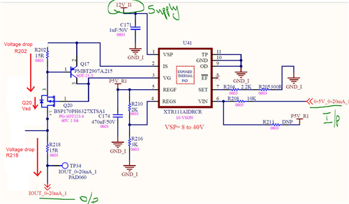
We are using the attached design for generating the 0-20mA from 0-5V input with Vsp-12V.

We got the results as per the calculation Iout-10*(Vin/Rset). For 0V- 0mA & 5V-20mA

But after 2 or 3 iterations the results are changed to 

For 0V- 2.6mA and 5V-25mA.

  • Hi sir,

    Yes sir...

    But I want clarification regarding Iout.

    Bcz I'm getting 2mA to 25mA instead of 0-20mA.

  • Hello M,

    What is the load resistance?  Is the load resistance referred to the same ground potential "GND_I" as XTR111?  Keep in mind the XTR111 is a three-wire current transmitter and the load resistance must be referred to the same ground potential of the XTR111.

    The XTR111 requires a minimum compliance voltage.  The XTR111 by itself, requires a minimum compliance voltage of 2V below the supply voltage VVSP. In addition, foot note (4) on page 3 states the XTR111 minimum compliance voltage is limited by (+VVSP -2V) + VDS, where VDS is the external transistor drain-to-source voltage required for linear operation of the external P-FET transistor.  We also need to account for the voltage drop of any series resistances in the output path, voltage drops due to external diodes/clamps on the current path.  See figure below.

     How many PCB/devices show this behavior? Are you measuring the current with a current meter or the voltage across a load resistor?  Please provide an schematic or diagram showing the load resistance and load resistance ground connections, and/or the current meter (or voltage meter) connections. 

    Thank you and Regards,

    Luis

  • What is the load resistance? 

    Load resistance is 220 Ohms.

    Is the load resistance referred to the same ground potential "GND_I" as XTR111? 

    Yes. GND_I is the ground potential for Load resistor.

    How many PCB/devices show this behavior?

    Two devices in the same board shows this behavior. 

    Are you measuring the current with a current meter or the voltage across a load resistor?

    Both methods we used for verifying the design. Present we are using the current meter to measure the current.

    Please provide an schematic or diagram showing the load resistance and load resistance ground connections,

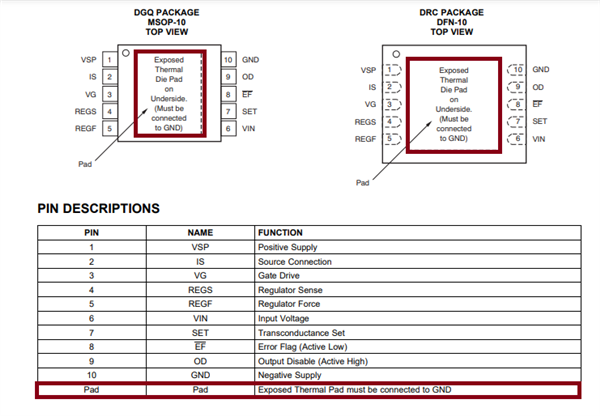
    And one more thing. If we didn't connect the Thermal pad to GND_I temporarily. is there any functioning error occurs in the design ?

    Pls clarify...

  • Hi Sandeep,

    Yes, you are correct.  The thermal pad must be connected to GND to ensure proper operation and biasing of the internal XTR111 circuits.  Issues will occur if the thermal pad is not connected to GND.  Please see below. 

    Thank you and Regards,

    Luis

  • Ok..

    In my design i'm using the 8-channels of XTR111 designs on same board.

    All are connected without Thermal pad to GND_I bcz of manual soldering issue.

    Ch-1- shows iout-2mA to 26mA from starting of my testing phase and then i changed the XTR111 IC now it is working Good.

    Ch-2- For 3 or 5 iterations i got 0mA to 20mA with this design after that i'm not getting the current output, We observed XTR111 IC pins 2 and 3 shows short connection.

    Ch-7- For 3 or 5 iterations i got 0mA to 20mA with this design after that it shows iout-2mA to 25mA.

    Remaining channels are working good.

    I'm attaching the my design pls verify.

    XTR111_8Channels.pdf

  • HI Sandeep,

    In order to avoid issues, please replace all XTR111 devices that were previously tested with the exposed thermal pad floating with fresh devices and ensure the thermal pad is grounded prior testing in all the new XTR111 devices.  These devices may have potentially been exposed to improper internal biasing and/or voltages above the max ratings when the thermal pad is disconnected. 

    After replacing the XTR111 devices, please ensure the boards go again through a proper flux cleaning process.  Flux often gets trapped underneath ICs where it can form undesired, parasitic capacitances and resistances.  These parasitic elements are may produce excessive leakage currents/drift on the circuitry, causing errors due to flux contamination. Consult the respective flux manufacturer or board assembly subcontractor, as proper flux removal may require use of a detergent based wash procedure.  For our lab PCB prototypes, we use a deionized water, an ultrasonic bath clean for 15 minutes, followed by a 75C oven bake-out for 30 minutes. The proper PCB cleaning process will depend upon the flux. type you use. 

    Beyond the issue of the unconnected thermal pad, I don't see differences as shown in the schematic between the different channels.  However, if you wish, we could review the board layout Gerber files.  

    Thank you and Regards,

    Luis  

  • Thank you sir...
    I'll update you the results once the new board is done with thermal pad connection.

  • Hi Sandeep,

    Thank you, will wait for your update

    Best Regards,

    Luis

  • Hi Sandeep,

    Let us know if you have additional questions.  If this thread is locked after a couple of weeks, please feel free to open a new query.

    Thank you and Kind Regards,

    Luis

  • Hi Sir,

    We want to share our data to you for verification of design related to above Query,

    Can you please share your personal mail id to us.

  • HI Sandeep,

    Per your request, I will contact you via private conversation. 

    Thank you and Regards,

    Luis