This thread has been locked.

If you have a related question, please click the "Ask a related question" button in the top right corner. The newly created question will be automatically linked to this question.

INA240: Common Mode Output Waveform

Part Number: INA240
Other Parts Discussed in Thread: REF3333,

Dear TI E2E-Team,

thank you for this greatly managed forum and your support. 

Currently we have a problem with the current sensing circuit of a PMSM motor drive board.
We are using three INA240A1 for sensing the phase currents inline:
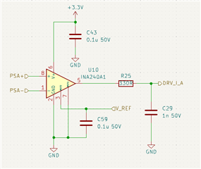
The PSA+ and PSA- are Kevlin connected to the shunt resistors and the DRV_I_A signal is connected to an ADC input. The V_REF input is taken directly from a REF3333 voltage reference. 

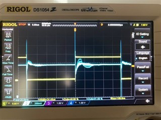
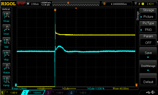
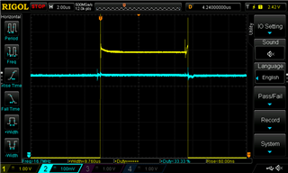
When driving the motor phases with 50% duty cycle and no load, we see the INA240 output behaving unexpectedly: Sometimes there are completly different signal waveforms:
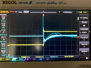
Channel 1, yellow: PSA- / Phase Output
Channel 2, blue: DRV_I_A / INA240 Output

The long settling time and strange waveforms make our ADC readings not usable. What are we experiencing here?

Thank you for your support.

Ben

  • Hi Ben,

    are you sure you want the REF voltage being as high as the supply voltage of INA240?

    Kai

  • Hi Kai,

    thank you for your reply.
    We've connected the external reference voltage as descriped in chapter 8.4.3.3 Output Set to Mid-External Reference. So the REF voltage would be 3.3V/2 = 1.65V, right?

  • Oh yes, sorry.

    Am I right that the common mode input voltage is a 100kHz square wave with an amplitude of 13V peak to peak and steep edges with a rise time of 30ns? I think you dynamically overrange the INA240. The INA240 is not fast enough to properly handle this fast common mode input signal.

    Kai

  • Hi Ben,

    What we’re seeing is predominantly interference of the switching common mode.

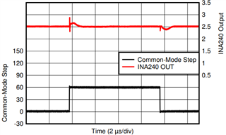
    However, with optimal layout, we should expect the output to settle to quiescent level in about 2uS. Here it is taking almost 10uS following a common mode rising edge. Besides, although spikes that coincide with the edges are expected, they are quite large given the common mode is <15V.  

    As a guidance, this plot shows the typical behavior:

    Some general best practices for this type of boards are - use multiple-layer, separate switching nodes from the rest of the circuitry, short return path for switching node recirculating current, partition planes to help guide switching current.

    I think if you fly-wire an INA240 in one of the phases, you'll probably see better performance, this experiment can help confirm if  it is layout related in deed.

    Regards, Guang 

  • Hi Guang,

    thank you for your reply.
    We were hoping for a performance like the plot in the datasheet. We're using a 4 Layer PCB; we have tried to keep the critical paths as short as possible. 
    Digital Ground and Power Ground are connected in a single point.

    The frequency of the PWM signal is 20kHz, the rise time isn't that fast (around 80ns). The graphs above were taken without any load / motor connected to the phases, so it's basically a "common mode rejection experiment". Do you have any idea what exactly the problem could be?

  • Hi Ben,

    Have all phases been checked to see if the behavior is consistent?

    I’m fully aware of the test condition. However I don’t know exactly where the issue lies. Though the most likely culprit is coupling, ie, the switching noise made to the output through a path outside the IC.

    We have a 48V BLDC motor drive ref design. In section 4.2.4, phase current transient response was reported. You may review to see what the performance is in a real-world example.

    Regards, Guang 

  • Hi Guang,

    thank you for your reply. Yes, the phenomenon can be observed on all three phases. This is already our second revision, our recent layout changes have not brought any improvement. 
    Do you have any suggestion where this coupling might likely take place? We are running out of ideas...

    Thank you very much for your help. 

  • Dear E2E-Team,

    we did some further measurements. The experiment is the same as above, no load connected and 20kHz PWM with 50% duty cycle.

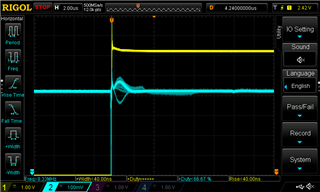
    It can be seen, that the INA240 output behaves differently whereas the input signal stays the same. The output waveform differs and there is a "slow" signal distortion after 5us...


    Here are two single shots:

     
    Do you have any ideas?

    Thank you.

    Kind regards,

    Ben

  • Hi Ben,

    These scope shots look much better and the disturbances settled much faster.

    Common mode disturbances take about 2uS to settle. Within the 2uS window, the waveform is not deterministic and can show up as either overshoot or undershoot. So the single-shot pictures look fine. This is also the reason for the delay needed after PWM transitions.

    For the persistence capture, there is one with a much longer tail (8uS total), I’m not sure what happened there. But if ADC sampling happens at 10uS or later, this shouldn’t be an issue, I assume?

    Sometimes, scope channel coupling can make signal looks worse. The chance is low, but it is probably worth making sure. Maybe you could measure INA240 output only (remove CH1) to see if it improves. Also try to shorten the scope ground wire, or wrap it around the probe.

    Regards, Guang 


  • Hi Guang,

    thank you again.
    The scope shots look better because of better grounding of the scope probe (spring) and only one phase is active. 
    Thank you about the clarification about the settling time waveform. We were just a little bit confused, because another hardware board of us that uses the INA240 (in PWR package) shows no such behavior...

    The problem is indeed the 8uS tail. We limit the duty cycle to take account of the 2uS settling time, but 8uS would be too much. And, sometimes the tail is even longer than 8uS. Do you have any idea, what's the reason for this behavior?

    We've checked INA's reference and supply pins, they're looking fine. 

    Regards, Ben

  • Hi Ben,

    I’m not sure exactly where the long tail comes from.

    Can you remove the shunt and short the input pins together? The best would be to short at the pins, but I understand this likely is not possible on a PCB. But try to make the short the best you can.

    This is a way to make sure the chip sees zero differential input even if there is some kind of stray current.

    Regards, Guang 

  • Hi Guang,

    thank you for your suggestion.
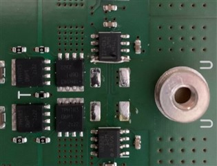
    We have desoldered the shunts and shortened the input pins together:

    This should make sure INA240 sees (nearly) zero differential input.
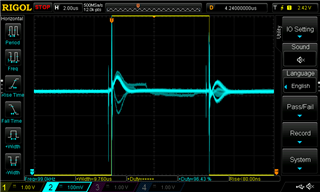
    However, the waveform with the long tail still persists:

    It shouldn't really be like that, should it?

    Regards, Ben

  • Now we removed the output filter resistance (R25) to eliminate any issues here. The INA240 differential inputs are still shortened. 
    We increased the gate resistance to aim for a slower rise time. 
    For the scope persistance capture shots, we increased the voltage amplitude / common mode voltage to 32V.

    The INA240 output signal (blue) is measured directly at the output pin, referenced to the ground pin with a spring probe.

    The other pins (ground, supply, reference) are all looking fine. The reference input pin for example:

    We have never experienced these issues before...
    Any help will be appreciated. 

  • Hi Benk,

    I would remove REF3333 for a test: Connect "REF2" of INA240 directly to "V+" of INA240.

    Digital Ground and Power Ground are connected in a single point.

    This can also be an issue. SIngle point grounding is not recommended with very fast signals. It may be better to use a solid ground plane.

    There is another issue: All the ground connections of INA240 should directly go to a ground plane. But I only see single vias.

    Also, where is the decoupling cap at pin 5 of INA240? This decoupling cap should sit closest to pin 5 and should also connect to the ground plane.

    Kai

  • Hi Kai,

    thank you for your response. 
    We have the board here with a single ground plane (last revision), but the waveform is the same here (at least with no load). 
    The digital ground plane is on layer 2, running directly underneath the INA240 pin, it can't be seen in the picture. The vias are connected to this plane.
    I'm not sure what you mean with the decoupling pin at pin 5 (pin 5 is the output pin in the SOIC package). We have 100nF decoupling caps on the supply voltage (pin 6) and voltage reference (pin 3). 

    As for the test without the REF3333: We will do your suggested test and post the results here.
    Thank you for your suggestions!

    Regards, Ben

  • Hi Ben,

    Is the behavior consistent across all phases, ie, can the long tail be observed on all? I wonder if the device itself is an outlier. After checking out the leads you’re currently pursuing, what about changing to a new device, or moving to another phase to see if the behavior follows the device?

    Meanwhile, try to measure the output only to see if it makes a difference, and trigger on the gate driver voltage which is much lower and less likely to cause crosstalk.

    Regards, Guang

  • Hi Guang, hi Kai,

    we've removed the REF3333 and used the 3.3V supply voltage as REF, but unfortunately the "long tail" is still persistent. 
    The behavior is consistent across all phases, we even have replaced the INA240's, but the waveform stays the same.

    We're wondering why the "long tail" appears only sometimes (as you see on the persistance capture shots). To rule out probing errors, we've reenabled the current sampling with the ADC's. As expected, we sometimes  see large measurement errors (the "long tail distorsion"). Normally, the ADC value has a noise of 2-3 LSB, when samplling closer to the swiching point, we get spikes at around 40-50 LSB. 
    We expect these spikes when sampling near the switching time + 2uS, but it starts already at around 10 uS, which corresponds to a duty cycle of about 40% @ 20kHz PWM. 

    In our last project, we used the INA240 in a multi-board configuration and these spikes started as expected at around < 10% duty cycle.
    Clearly, we seem to be doing something wrong here, but we can't find the error...

    Regards, Ben

  • Hi Benk,

    I'm not sure what you mean with the decoupling pin at pin 5 (pin 5 is the output pin in the SOIC package).

    Yes, correct, was a typo.

    The way the two inputs are connected to each other (short-circuit) may not be symmetrically enough for the very steep edge and the common mode signal may partially transform into a differential signal at the inputs of INA240.

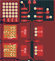
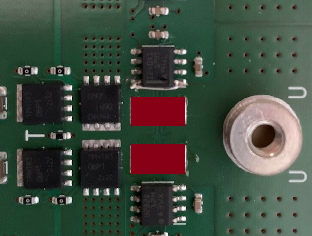
    I would try to optimize the short-circuit like shown below (by soldering zero Ohm shunts or thick copper wires at the places where the shunts have to be soldered) and would remove the piece of wire between the two inputs:

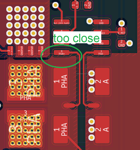
    Also, even with the original shunts soldered onto the printed circuit board, the upper shunt may be too close to the INA240. The common mode signal may capacitively couple into the both inputs of INA240 unevenly, resulting in a differential input signal, making it for the INA240 impossible to fully remove the common mode input signal.

    So, I would try to move the INA240 a bit away from the two shunts and eventually shield the inputs of INA240 by a piece of ground plane between the shunts and the inputs of INA240:

    Kai

  • Hi Kai,

    thank you very much for your valuable advice regarding the hardware layout.
    We were trying to get the INA240 as close as possible to the shunt resistor, in this case it might be a bit too close then.
    What we are surprised about is that we see this "slow" signal distortion long after the actual switching process. Is this typical for capacitive coupling?

    We will incorporate the suggestions into the next hardware iteration and post the results here.

    Thanks again for your help.

    Kind regards, Ben

  • Benk,

    Guang is out of the office at the moment, so I thought I would try and assist here. I agree with Kai that there could potentially be coupling present here, and a bit more separation could potentially help here. I also question for the size and timing of the pulses if perhaps there could be due to the small added inductance on the nodes due to the amount of vias present in the stitching. It's most likely fine but just trying to brainstorm other potential avenues of exploration for this behavior. 

    Please keep us abridged and let us know how the testing you mentioned goes. 

  • Hi Benk,

    to find out how good the INA240 can suppress your 20kHz common mode input signal, I would build a test circuit with the INA240 and give to it inputs 20kHz square waves with different rise and fall times from a function generator.

    I would play a bit with the layout of the test circuit to see the effect of the solid ground plane and how the INA240 behaves when the layout becomes less and less ideal.

    Divide and conquer!

    Kai

  • Hi Ben,

    Just a bit more info for future reference:

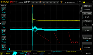
    Here is a persistence scope capture taken a few years back during product characterization. The condition for this particular graph was – PWM common mode (amplitude 60V, frequency 50KHz, duty 20%).  PWM was generated by a GaN driver (<10nS rise/fall time). The persistence capture shows no long tails.

    I’ll close the thread for now, but feel free to let us know of further findings.

    Regards, Guang