This thread has been locked.

If you have a related question, please click the "Ask a related question" button in the top right corner. The newly created question will be automatically linked to this question.

OPA2188:OPA2188: RTD linearizzation

Part Number: OPA2188
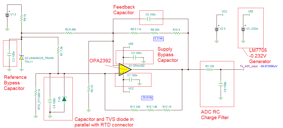
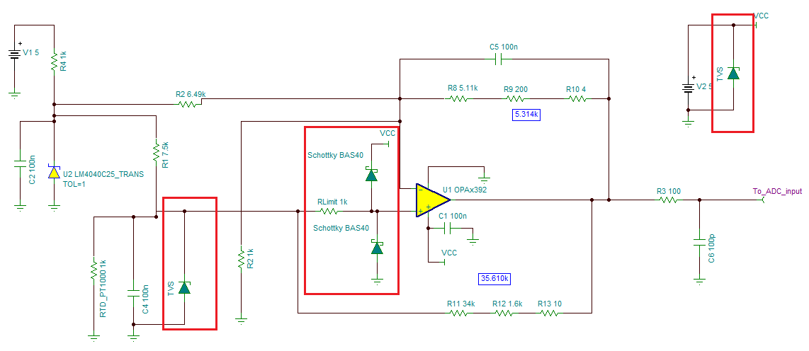
Other Parts Discussed in Thread: ADS1262, ADS1261, ADS1248, LM7705, OPA2392, LM4040, ADS1118, ADS1113, ADS1115, ADS1114

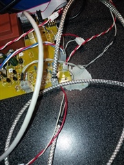
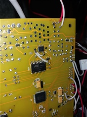
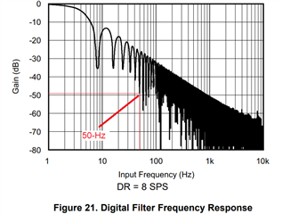
On the basis of OPA2188, I also carried out linearization according to the slyt442.pdf manual, LM 4040A 2.5 acted as a reference signal. ADCs represented the Atmel family of microcontrollers - Attiny 261A and Atmega32A. I will say right away that everything is correct, everything works, there are no complaints about the scheme. But unfortunately, the data obtained after the ADC conversions do not stand up to scrutiny. Despite the fact that all elements (resistors, REF) are selected with an accuracy of 0.1%, the temperature readings change in an incomprehensible way. 22 degrees Celsius, then it can be 25 C, then again 22, then again 22, 21, 23,22,24 and so on with time intervals no matter what (at least 0.1 s, at least 1 s, at least 2 s and so on ) in an environment in which the temperature does not change much - I sit in a room at a computer. I didn't even try to indicate tenths of a degree. Instead of Pt1000A, I tried soldering a regular resistor of about 1.1 kOhm into the board. The readings stopped changing. I got busy with the wires to this sensor, I tried a shielded audio cable - it helped a little, but the readings still changed. I encased the sensor in a metal sleeve and added a new shielded copper braid. Which I connected to GND through a 0.1 uF capacitor. Unfortunately it didn't get any better! Full shielding, but useless, as it turned out. There are no powerful or not powerful household or industrial devices nearby, the computer can be turned on, or it can be turned off - it doesn’t matter. For power, a 10 uF tantalum capacitor, for AREF also a 10 uF tantalum capacitor, plus a 0.1 uF ceramic capacitor here and there. The location of the elements on the edge of the board away from the power rails. This is some kind of nonsense. A low-noise op amp outputs this noise to the ADC. The voltmeter shows an alternating voltage from 6 to 18 mV at the output of the opamp, but as I understand it, the peaks can be more significant. As I understand it, the mains voltage of 50 Hz and its harmonics gives interference, I read that, for example, the MAX31865 has a special filter "50 / 60Hz DIGITAL SINC FILTER", which dampens this noise by 40 dB. And how are things in OPA2188? What should I do? I've already tried everything. I have three different printed circuit boards of the sample assembled on them and everywhere a similar situation. For example, the ADC conducts 4 samples and compares the highest 8 bits for the same data and then only skips the data further, and if there is an error, then repeated measurements and so on several times. In general, this is not the case. What else can I do? The ADC inputs were converted to analog inputs, the ADC was both with and without sleep mode. Maybe you need some kind of load resistor and (or) capacitor for the output of the operational amplifier? Help me please.

  • Hi Serhii,

    Can you please provide a full-schematic of the circuit above? 

    How long are the connections between the amplifier and RTD probe? Is there an RC filter at the output of the amplifier between the ADC and op-amp circuit?  Is the ADC the Atmega32A? What is the sampling rate, acquisition time and sample-and-hold capacitor of this ADC? Is this a 10-Bit SAR ADC? 

    You are correct that 50-Hz and 60-Hz power line noise tends to dominate on RTD measurements.  Most precision, high-resolution, 24-Bit Delta-Sigma converters that are optimized for RTD measurements offer digital filters to eliminate noise.  The  ADS1262, ADS1248, ADS1261 are examples of Delta-Sigma ADCs incorporate digital filters with notches at these 50-60Hz line noise frequencies to greatly attenuate this noise.  Another technique that can is used to eliminate line noise is to sample through a complete line cycle and average several samples through the line cycle period.  Just as an example, a 16-bit precision SAR ADC could be set to sample at 3-kSPS, and average 50 samples during a 16.6ms period to help reduce 60-Hz noise, or similarly sample at 3-kSPS and average 60-samples during a 20-ms period to reduce 50-Hz power-line noise.  Keep in mind, the ADC DC accuracy, and resolution, as well as noise and accuracy of the ADC voltage reference will directly affect the overall system noise and accuracy.

    The OPAx188 is a zero-drift (chopper) amplifier, and relatively subtle errors can occur when the inverting and non-inverting terminal input impedances are un-matched.  When using chopper amplifiers, I tend to attempt to match the equivalent input impedances on the inverting and non-inverting terminals.  Nevertheless, I suspect the large errors you describe point to other problems related to noise or stability, or ADC drive.  We can provide suggestions that are related to the OPA2188 circuit, but may not be able to answer questions specific to the Atmega32A.

    A complete schematic and layout information will be helpful.  

    Thank you and Regards,

    Luis

  • Good afternoon.
    Answers on questions:
    I present two schemes of my devices. In one of them, all processes are processed by Atmega 32A, including the ADC (10 bits, but I use only the upper 8 bits, 0.5-1 degrees Celsius accuracy is enough for me), in the second scheme, I specifically used a separate chip for the Attiny 261A ADC, so that you can put this chip into sleep for more accurate ADC readings and make the ADC inputs analog (register DIDR). ADC sampling rate 62500 Hz (8MHz/128 within 50-200kHz as required by Atmel) for the second circuit (more complex). From time to time, processed data is transmitted from 261A to 32A via SPI and displayed in turn. As I have already said, data processing at the ADC input is carried out according to the algorithm for continuous measurement of 4 readings, and if they match in the upper 8 bits, the data is recorded. If there is no match, the process of measuring 4 values in a row goes on again and so on. Until they match. Or the limit is reached. I tried a lot of things at the program level, including averaging - I took 1024 matching samples (in 4 dimensions, as I said), summed it up and divided by 1024. But still every second or two the readings were unstable. I spent many months on this and other things, and even years, but alas! Therefore, I am writing to you.
    Now the length of the wires from the board to the sensor is 1.2 m. The resistance of the wire of one is 0.6 m, the other, respectively, too (2-wire circuit). Shielding gave a significant effect, but very insufficient.
    There is no RC chain filter, I’m just thinking about it, but I don’t understand how to arrange it so that it extinguishes both 50 Hz and harmonics (100, 200, 400 Hz at least). Please advise me how to set it up.
    Regarding your advice on sampling, I understand that you need to try to make measurements in the entire range from the beginning of the 50 Hz sinusoid to its end, and then average my readings?
    Maybe I'm somehow not connecting the shielded wire from the sensor?
    Looking forward to your answers! Thank you very much for responding!!!  Schematic_KE-Atm32-Att261_2023-02-22.pdfSchematic_SO-Pl1_2023-02-22.pdf

  • Hello Serhii,

    I have a couple recommendations on the OPA2188 circuit portion:

    Op-amp output swing and bipolar supplies reach 0V:

    I assume the OPAx188 circuit output is required to reach 0V when the RTD=1000Ω (0°C). However, in the schematic, the device is powered with a unipolar supply with (V-) connected to GND.

    Because no Op-Amp can reach all the way down to 0V in a single supplied circuit, you need a small negative supply voltage. The OPAx188 amplifier output requires more than > ~270mV headroom from the negative rail. The most conservative open-loop (AOL) specification specifies output swing of 500mV from the rail supplies.  If you need this op-amp to reach ~0V, you will need a small negative supply of -500mV for the OPAx188 supply.

    Another option is to select the OPA2392 (5.5V max supply amplifier), and use the LM7705 (-0.232V) negative bias generator to generate a negative supply. The conservative OPA2392 AOL output swing requires a smaller ~100mV from the supplies; and the LM7705 generator is sufficient.

    One possible circuit with the OPAx392 circuit is below: 

    NOTE:  I copied the resistor values from your schematic. I assumed you are using the SLYT442 application note excel calculator to obtain the resistors values.  If you let me know the output voltage targets, the PT-1000 temperature range and the op-amp (V+) supply voltage, I can verify the resistor components.

    RC filters at the circuit input and feedback:

    There are no filters at the input of the amplifier circuit or in the signal path to limit noise.  I suspect the circuit may be prone to EMI interference/noise.  One suggestion is to add a 100nF capacitor in parallel with the RTD connector to filter high frequency input noise.  You could also apply a matching feedback capacitor as shown above. Also, consider adding a TVS or Zener diode for protection at the RTD connector.

    Supply Bypass / Reference Bypass Capacitors:

    Please use local 100nF bypass capacitors on the op-amp positive (V+) and negative supplies (V-).  The bypass capacitors need to be place in close proximity to the op-amp supply pins.  Similarly, you could consider using a bypass capacitor in parallel with the LM4040 reference.

    RC low-pass / charge kickback filter at the ADC inputs:

    I don’t have detailed information about the ADCs since they are from another manufacturer; however, you 'could' consider placing a RC low-pass filter such as 100-Ω and 100pF capacitor right at the ADC input to help filter any high frequency external noise.

    General PCB layout and grounding recommendations:

    Below are key/general PCB layout recommendations, just FYI:

    • The ground scheme on the PCB layout plays a pivotal role when eliminating errors due to noise/EMI. These days, our most common recommendation is to use a single solid ground layer underneath the devices, but it is important to partition the board in analog and digital sections. 
    • In general, we recommend a single ground plane while partitioning the board or essentially keeping the placement of the digital and analog portions of the circuit on separate areas on the PCB, keeping the sensitive analog away from noise sources and digital signals.  Although the PCB board layout uses a single GND plane, the key is to keep the current return paths on different sections of the board layout.  The return currents tend to travel right underneath the signal trace, and the key is to keep these signal paths separate.
    • Partition the board in two areas, keeping the sensitive analog input signals away from the digital signals.  The reference decoupling components and analog inputs are kept away from the switching digital signals. This arrangement prevents noise generated by digital switching activity from coupling to sensitive analog signals.
    • The power sources, and reference pins of to the device must be clean and well-bypassed. Use ceramic bypass capacitors in close proximity to the analog and digital power-supply pins. If possible, place all bypass capacitors on the same top layer of the devices.  Avoid placing vias between the analog and digital supply pins and the bypass capacitors. Connect all ground pins to the ground plane using short, low impedance paths and independent vias.  Also use independent vias to connect each bypass capacitor to GND.
    • The ADC input RC charge kickback filters are placed immediately next to the ADC input pins, ideally in the same layer as the input device pins.

    Regarding the 50-Hz power line noise, one common recommendation is to average samples during the 20-ms power line cycle, as we have discussed above; or use an ADC with a digital filter providing attenuation notches at 50-Hz (or 60-Hz).

    Thank you and Regards,

    Luis

  • Good afternoon Luis.
    Thank you very much for the answers and for the modern scientific lecture on PCB layout. I have never used a solid copper layer, now I will try. Maybe you have a similar sample to see examples? But basically I get it. I tried to adhere to many of the rules you described, but as I see not all of them, I will rebuild to the correct wiring. In my samples, I used two grounds GND and AGND, which I connected at one transition point. Now I understand that a solid ground layer will exclude analog and digital ground separately?
    I also want to say that my device will not work at a temperature of 0 degrees Celsius. I care about room temperature and up to 127 degrees Celsius or 180 or 260. So I don't think I should bother with a negative voltage source?
    Thank you very much for the advice on averaging readings over 20ms, I hadn't thought of that in all this time. I will definitely do it. As for checking the circuit elements, I think that everything is correct, since when the water boils it shows 100 degrees Celsius (+ - my interference). I will implement your advice step by step and after all this I will definitely write here if you do not close this topic.
    I also forgot to ask why the TVS diode? What is his mechanism of work in this case. I also wanted to ask you, maybe you know why LM 4040A, designed for an output of 2.5 Volts, shows 2.470 in approximately all of my samples, although I tried different values ​​of resistors to limit currents. I have a good voltmeter. I never understood. An accuracy of 0.1% should not allow such a deviation. Here comes out 1.2%!!! Some kind of disgrace.

  • Hi Serhii,

    I have suggested general info/layout recommendations and mentioned grounding considerations since we are discussing noise. There are different approaches to PCB layout, and the design with split GND layers can work as well. There is a tendency these days to recommend the use a single ground layer due to EMI considerations, since in many applications mixed analog digital boards need to pass intensive CE testing. In some cases, it may be hard to make a board pass the CE tests when using a narrow connection in the two split ground planes to each other. That said, there may be applications that also have strong reasons to favor the split GND level approach and this approach can also work as well.  However, the PCB layout decision depends on the application requirements; and it is the designer’s preference. When using the single ground layer approach, you still partition the board into analog and digital sections. There is a discussion about this topic in the post below:

    https://e2e.ti.com/support/data-converters-group/data-converters/f/data-converters-forum/755516/faq-pcb-layout-guidelines-and-grounding-recommendations-for-high-resolution-adcs

    There is a tutorial/presentation on EMI/PCB layout tutorial on the TI Precision Labs section below that may be of interest regarding mixed-signal designs:

    https://training.ti.com/ti-precision-labs-introduction-pcb-design-for-good-emc

    https://training.ti.com/zh-tw/pcb-layout-0

    You are correct. If your design does not require reading cold temperatures, or the op-amp output is not required to reach ~0V, you do not need to worry about the negative supply.  The OPA2188 is a zero-drift, chopper amplifier.  Chopper amplifiers can be sensitive to large impedance mismatches at the inverting and non-inverting inputs, although I should highlight that these errors tend to be subtle. The equivalent impedances in the design are not far mismatched, but adding the capacitors at input/feedback above will help. If your op-amp supply is <5.5V, the OPA2392 is a linear (non-chopper) that could also serve you well, it also offers relatively low offset drift as well; and the offset error/drift of the op-amp is not a dominant error when using a10-bit level resolution ADC.

    In your application, if the non-inverting op-amp input terminal of the op-amp is exposed or can be accessed through the RTD connector to the external environment, it may be possible that the amplifier can be exposed to ESD events. The TVS diode was a quick attempt to protect the devices for any overvoltage/overcurrent conditions or ESD events. A better method may be to use Schottky diodes, ensuring the inputs do not exceed the AVDD supply voltage by more than a few 100s of millivolts.   In this example, the BAS40 is a small-signal Schottky diode with a forward voltage close to ~380 mV at 1 mA. In comparison, the op-amp internal ESD structure has a forward voltage of ~550 mV at the same forward current. Therefore, the Schottky diodes turn on before the amplifier’s internal ESD diodes, and most of the in-rush current flows through the external clamp. The internal ESD structure can only withstand 10 mA, while the external Schottky diode can handle forward continuous currents up to 200 mA, providing a robust level of protection. A TVS diode on the supply can be used to sink current.

    In your design, you could use a combination of Schottky diodes and TVS supply protection as shown below; however, this only applies if the amplifier input will be exposed to ESD or overvoltage in the application.


    There is more information on how to select TVS and Schottky diodes on the resources below.

    https://training.ti.com/ti-precision-labs-op-amps-electrical-overstress-introduction

    Not sure about the issue is with the LM4040A25 reference issue.  This one is specified for current at current ~100uA, and ±2.5mV tolerance at 25C and ±19mV across -40C to 85C.  Changing the current, as long as inside the specified current range should not change the voltage to 2.47V.  Are you measuring the voltage right across the pins of the shunt reference? or in reference to other GND point? Can you place an oscilloscope probe to check for any unwanted AC signals/oscillations?  

    Thank you and Regards,

    Luis

  • HI Serhii,

    One suggestion on the LM4040A25 is to check for any unexpected AC signals / noise using an oscilloscope.  Also add a parallel or load bypass capacitor. 

    The datasheet recommends a 0.1μF, low ESR, Ceramic bypass capacitor.  If possible, use X7R-grade with 10V or 16V rating.

    Thank you and Regards,

    Luis

  • Hi Serhii,

    I have not heard from you; however, if you have further questions, please feel free to post.

    Thank you and Kind Regards,

    Luis

  • Greetings, Louis. I'm going with my thoughts now to ask new questions. I have already converted a lot in the scheme and on the printed circuit board, respectively. This really gave a very good positive effect. You are just a wizard. I have not yet set the TVS diode (I'm waiting for when I come to me), then I will also inform you. Then I rewrote the program for 64 samples of the ADC testimony within 20 ms. This also helped a lot. Unfortunately, I can’t remake the printed circuit board itself for a long time so that there is a continuous grounding. If I understand you correctly, is it better to make grounding on both sides of the printed circuit board? Now, as I said, the indications within one degree of Celsius practically do not change, but depend on the time of day. For example, late in the evening - at night smaller interference. And in the evening there is more interference. In general, I will write in this topic soon. I hope everything will work out, and if not, you will advise me some specialized ADC with the filtration of interference for acceptable money?)))

  • I apologize for incorrectly wrote your name Luis!

  • HI Serhii,

    I am glad to hear that the measurements are improving! Happy to help.

    Regarding  Delta-Sigma ADCs providing attenuation at 50-Hz or 60-Hz, the ADS1113 / ADS1114 / ADS1115 are 16-Bit, I2C interface devices providing attenuation around -45dB ~@ 50-Hz. The ADS1118, 16-Bit, SPI interface is another possibility.  There are other higher resolution devices offering better filtering attenuation.

    However, if you are primarily interested on the 12-bit resolution / lower cost options providing this digital filtering capability, it is best to submit a query on the E2E on the Data Converters Forum; and ask the ADC Applications team experts as they have in depth knowledge of the ADC portfolio.  

    E2E Data Converters Forum:

    https://e2e.ti.com/support/data-converters-group/data-converters/f/data-converters-forum

    Thank you and Kind Regards,

    Luis

  • Hello Luis.
    I can’t tell you for sure whether the TVS diode helped me or not, but at least, since it is needed, then let it be. I'm already completely confused. As I wrote earlier, everything very much depends on the load on the electrical network. The picture is as follows: the readings are very stable at night, when everyone is sleeping and quite unstable, for example, during the day, in the evening. At the same time, I measured the mains voltage and it does not change much when inaccuracies in the readings occur. I even tried to place the sensor at a very short distance from the place of its contact on the board - it did not help either. I made a program to see not only degrees, but also 0.5 degrees Celsius. And I can say that when there is silence on the network, the data does not change the readings for tens of minutes: 23.5, 23.5, 23.5 ... 23.5, etc.
    But when the network is noisy, it can be half a minute - a minute to be 23.5, and then a minute - two 23.0, 24.0, 25.0, 23.0, etc. I even tried to put an EMI filter. Did not help. I understand that grounding does not affect here, because then the nature of the interference would be more or less predictable. Now I think, since even with a short wire to the Pt1000 sensor, the nature of the errors does not change, it turns out that everything comes through my power supply. I don’t know if I did it right, that after the rectifier and L7805 I put a 4700 microfarad capacitor?
    I posted a query about a delta sigma ADC today on the forum. It is a pity that for all my efforts nature put me in my place!)))

  • Hello, Luis.
    Perhaps I hastened to say that at night the readings do not change. That night I left the device turned on and realized that the board lives its own life. The readings are unstable all the same, at times the temperature deviates as she wants by 1-2 degrees Celsius. So the reason is not completely clear, it is possible, after all, and as you said that the wrong non-continuous grounding is to blame. Just to understand this, you will have to spend a lot of time and money to redo it and assemble it again. But where is the guarantee that my temperature instability will not happen again? Probably better to go straight to the delta sigma ADC section? What do you think?

  • Hey Luis.
    You did not have time to answer me, and I am already writing again on the same day. Today is my creative day! This is entirely your merit. Thank you very much, I wish you all the best and hope that my cooperation with your company will be even more active and fruitful! Today I devoted the whole day to my problem and as a reward I found an inaccuracy in my program for obtaining ADC data and averaging readings. I forgot to invalidate the result after averaging the readings and it constantly overlapped, albeit slightly, with the following results. After correcting this error, I did not expect any significant positive, but everything fell into place! The readings are perfect, I decided to try to increase the resolution of the readings to 0.5 degrees Celsius - everything is clear, without interference. No jumps, no problems! I put the sensor with the usual twisted wires without a screen and again everything is perfect! I tried 9 bit precision, which is 0.25 degrees Celsius. Almost perfect. And all this at any time, even during peak hours, even at night, it doesn’t matter. I'm just in shock. I did not expect such a result! How much pain in the past. Now I can start mass production of my product.
    I need one more piece of advice from you. Maybe you can guide me: I need to organize the protection of power devices (triacs) from short circuits of heating devices (heating elements). There are many heaters, 3,6,9 or 12. The power of each is 3-3.5 kW. I thought to put shunt resistors to ground, but with a resistance of 0.1 ohms, a power dissipation of 23 watts is obtained. It's too much, of course. If the shunt is set to 0.01 Ohm, then 2.3 W, it seems to be nothing, but the voltage from it will be only 0.15 volts of alternating voltage, which must also be turned into a constant one, and the rectifier diode will not help. He'll eat all that stress, you know. I’m already silent that now all the heating elements are turned on by a triangle (220/380 V), here the shunts will not help either. I can put heating elements on 230 volts with a neutral wire, as I wrote above, but this will increase the triac currents and the reliability of the heating elements. And putting 6, 9 or 12 current transformers will be quite expensive. Can you direct my thoughts in the right direction? Does TI have solutions?

  • HI Serhii,

    That's great news. I am glad the noise measurement issue with the OPA2188 and SAR ADC was improved or has been resolved. Thank you for the update and letting us know. 

    Regarding the question about the protection of the triac power devices, this would be outside my area of expertise.  The sensor and/or current sensing applications team may be able to offer suggestions. Since this is a new topic, please start a new thread, providing the relevant schematic and/or block diagram details to the Sensors forum, and the current sensing applications team may be able to offer suggestions or point you in the right direction.

    Thank you very much,

    Kind Regards,

    Luis