This thread has been locked.

If you have a related question, please click the "Ask a related question" button in the top right corner. The newly created question will be automatically linked to this question.

INA826: Temperature drift of INA826

Part Number: INA826

Hi Team,

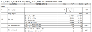
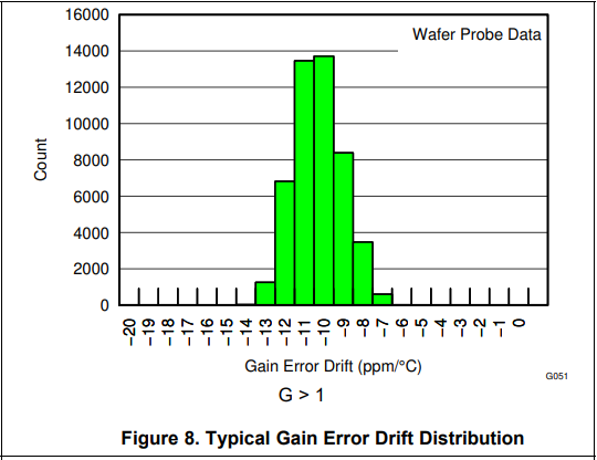
One question about the temperature drift of INA826. On this page what is the test condition? why the gain error drift is all negative in this diagram?

Also when Gain>1 will the temp drift highly related to the shunt resistor ? My customers have high requirement on temp-drift so they would like have some insight from you, thanks!
Manu Chang

  • Hi Manu,

    The test condition is Vs = ±15V, RL = 10kΩ, Vref = 0V.

    These charts show what a typical distribution of parts will look like. Of course, process variations and different wafer batches can produce gain error drift that is either positive or negative. It is likely that the distribution shown contains devices from a single wafer which shows the distribution around the typical value of 10ppm/°C, in this case negative. You may refer to the electrical characteristics section of the datasheet for the typical and maximum gain vs temperature drift specifications. The max specification is the "worst-case" error that can present in a device, however the vast majority of devices will have errors distributed around the typical value similar to what is shown in figure 8.

    The datasheet specified values for gain error do not include the effects of the external gain-setting resistor, Rg. The gain errors specified in the datasheet are very low due to the precision laser-trimmed internal feedback resistors. For G>1 applications, the resistor tolerance and temperature coefficient of Rg must be considered as these errors will contribute to the total gain error of the circuit.

    Regards,

    Zach